SGLS121E July 2002 – April 2025 UCC2800-Q1 , UCC2801-Q1 , UCC2802-Q1 , UCC2803-Q1 , UCC2804-Q1 , UCC2805-Q1
PRODUCTION DATA
- 1
- 1 Features
- 2 Applications
- 3 Description
- 4 Device Comparison
- 5 Pin Configuration and Functions
- 6 Specifications
-
7 Detailed Description
- 7.1 Overview
- 7.2 Functional Block Diagram
- 7.3
Feature Description
- 7.3.1 Detailed Pin Description
- 7.3.2 Undervoltage Lockout (UVLO)
- 7.3.3 Self-Biasing, Active Low Output
- 7.3.4 Reference Voltage
- 7.3.5 Oscillator
- 7.3.6 Synchronization
- 7.3.7 PWM Generator
- 7.3.8 Minimum Off-Time Setting (Dead-Time Control)
- 7.3.9 Leading Edge Blanking
- 7.3.10 Minimum Pulse Width
- 7.3.11 Current Limiting
- 7.3.12 Overcurrent Protection and Full Cycle Restart
- 7.3.13 Soft Start
- 7.3.14 Slope Compensation
- 7.4 Device Functional Modes
- 8 Application and Implementation
- 9 Device and Documentation Support
- 10Revision History
- 11Mechanical, Packaging, and Orderable Information
Package Options
Refer to the PDF data sheet for device specific package drawings
Mechanical Data (Package|Pins)
- D|8
Thermal pad, mechanical data (Package|Pins)
Orderable Information
7.3.4 Reference Voltage
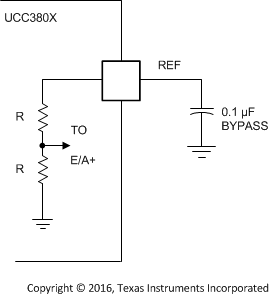
The traditional 5-V amplitude bandgap reference voltage of the UC3842-Q1 family can be also found on the UCC2800-Q1, UCC2801-Q1, UCC2802-Q1, and UCC2804-Q1 devices. However, the reference voltage of the UCC2803-Q1 and UCC2805-Q1 device is 4 V. This change was necessary to facilitate operation with input supply voltages below 5 V. Many of the reference voltage specifications are similar to the UC3842 devices although the test conditions have been changed, indicative of lower-current PWM applications. Similar to their bipolar counterparts, the BiCMOS devices internally pull the reference voltage low during UVLO, which can be used as a UVLO status indication.
 Figure 7-4 Required Reference Bypass
Note that the 4-V reference voltage on the UCC2803-Q1 and UCC2805-Q1 is derived from the supply voltage (VCC) and requires about 0.5 V of headroom to maintain regulation. Whenever Vcc is below approximately 4.5 V, the reference voltage also drops outside of its specified range for normal operation. The relationship between VCC and VREF during this excursion is shown in Figure 7-5.
 Figure 7-5 UCC2803-Q1 REF Output vs VVCC
The noninverting input to the error amplifier is tied to half of the PWM's reference voltage, VREF. Note that this input is 2 V on the UCC2803-Q1 and UCC2805-Q1 and 2.5 V on the higher reference voltage parts: the UCC2800-Q1, UCC2801-Q1, UCC2802-Q1, and UCC2804-Q1.