SLUSD37E October 2017 – November 2019 UCC28056
PRODUCTION DATA.
- 1 Features
- 2 Applications
- 3 Description
- 4 Revision History
- 5 Device Comparison Tables
- 6 Pin Configuration and Functions
- 7 Specifications
-
8 Detailed Description
- 8.1 Overview
- 8.2 Functional Block Diagram
- 8.3
Feature Description
- 8.3.1 CrM/DCM Control Principle
- 8.3.2 Line Voltage Feed-Forward
- 8.3.3 Valley Switching and CrM/DCM Hysteresis
- 8.3.4 Transconductance Amplifier with Transient Speed-up Function
- 8.3.5 Faults and Protections
- 8.3.6 High-Current Driver
- 8.4 Controller Functional Modes
- 9 Application and Implementation
- 10Power Supply Recommendations
- 11Layout
- 12Device and Documentation Support
- 13Mechanical, Packaging, and Orderable Information
Package Options
Mechanical Data (Package|Pins)
- DBV|6
Thermal pad, mechanical data (Package|Pins)
Orderable Information
8.3.1 CrM/DCM Control Principle
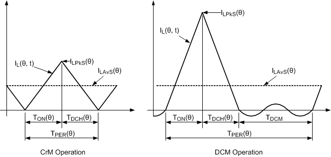
 Figure 19. PFC Inductor Current Waveform for CrM and DCM Operation
 Consider a single switching cycle that occurs at angle (θ) during the Line Cycle. Assuming ideal CrM operation the average inductor current (ILAvS(θ)) that flows during the switching cycle is given by:

A fixed circuit has constant inductance (LBST), so if the switch ON duration (TON(θ)) holds constant (TON) , across the Line Cycle, then the average input current remains proportional to the input voltage. In other words, when controlled in this way, the Boost converter behaves as a resistive load (RInEq) connected across the Line.

the next step is to consider DCM operation. Equation 3 describes the average inductor current that flows during the switching cycle.

To ensure average input current proportional to input voltage it is necessary for the on-time product TON(θ) x δONDCH(θ) is kept constant across the Line Cycle. Equation 4 shows the equivalent input resistance.

The minimum effective input resistance (RInEqMin) is needed to draw maximum power (PInMax) from minimum Line voltage (VInMinPkL):

Assume that full power operation at minimum Line operation is in CrM mode. Use Equation 6 to calculate the PFC inductor value required to deliver maximum power from minimum Line.

where
- TONMAX0 is the maximum switch ON time
Input power demand is an expression of the ratio of input power over maximum input power.

Equation 8 rearranges Equation 7 to express TON(θ) time as a function of power demand.

Equation 8 represents the CrM/DCM TON control principle implemented by UCC28056. This equation is quadratic in nature but UCC28056 employs the value of δONDCH(θ) from previous cycles as the basis for computing TON(θ) for the current cycle. The process is similar to solving an equation numerically by iteration.
A range of operating frequency options are available for CrM/DCM light-load operation. At one extreme, it can operate at high frequency with low current pulses in CrM mode (TDCM = 0). At the other extreme it can operate, in DCM mode, at minimum frequency (TDCM = TDCMMax) with current pulses of maximum amplitude. The controller can select a TDCM value anywhere between these two extremes. Conduction loss normally dominates when operating at minimum operating frequency leading to reduced efficiency. Switching loss normally dominates when operating at maximum operating frequency (CrM) also leading to reduced efficiency. Typically the most efficient operating frequency occurs when the pulse current amplitude is approximately one third of the maximum value.


The UCC28056 transitions from CrM to DCM operation when the peak inductor current across a Line Cycle drops below ILPkSOpt. While in DCM operation it adjusts the switching frequency to ensure that the peak inductor current across a Line Cycle remains close to ILPkSOpt for all Line and Load conditions. In this way, UCC28056 attempts to maximize efficiency for all loads and for all Line voltages.