SLUSD37E October   2017  – November 2019 UCC28056

PRODUCTION DATA.  

  1. Features
  2. Applications
  3. Description
    1.     No Load Power
      1.      Device Images
        1.       Simplified Application
  4. Revision History
  5. Device Comparison Tables
  6. Pin Configuration and Functions
    1.     Pin Functions
  7. Specifications
    1. 7.1 Absolute Maximum Ratings
    2. 7.2 ESD Ratings
    3. 7.3 Recommended Operating Conditions
    4. 7.4 Thermal Information
    5. 7.5 Electrical Characteristics
    6. 7.6 Typical Characteristics
  8. Detailed Description
    1. 8.1 Overview
    2. 8.2 Functional Block Diagram
    3. 8.3 Feature Description
      1. 8.3.1 CrM/DCM Control Principle
      2. 8.3.2 Line Voltage Feed-Forward
        1. 8.3.2.1 Peak Line Voltage Detection
      3. 8.3.3 Valley Switching and CrM/DCM Hysteresis
        1. 8.3.3.1 Valley Delay Adjustment
      4. 8.3.4 Transconductance Amplifier with Transient Speed-up Function
      5. 8.3.5 Faults and Protections
        1. 8.3.5.1 Supply Undervoltage Lockout
        2. 8.3.5.2 Two Level Over-Current Protection
          1. 8.3.5.2.1 Cycle-by-Cycle Current Limit Ocp1
          2. 8.3.5.2.2 Ocp2 Gross Over-Current or CCM Protection
        3. 8.3.5.3 Output Over-Voltage Protection
          1. 8.3.5.3.1 First Level Output Over-Voltage Protection (Ovp1)
          2. 8.3.5.3.2 Second Level Over-Voltage Protection (Ovp2)
        4. 8.3.5.4 Thermal Shutdown Protection
        5. 8.3.5.5 Line Under-Voltage or Brown-In
      6. 8.3.6 High-Current Driver
    4. 8.4 Controller Functional Modes
      1. 8.4.1 Burst Mode Operation
      2. 8.4.2 Soft Start
  9. Application and Implementation
    1. 9.1 Application Information
    2. 9.2 Typical Application
      1. 9.2.1 Design Requirements
      2. 9.2.2 Detailed Design Procedure
        1. 9.2.2.1 Custom Design With WEBENCH® Tools
        2. 9.2.2.2 Power Stage Design
          1. 9.2.2.2.1 Boost Inductor Design
          2. 9.2.2.2.2 Boost Switch Selection
          3. 9.2.2.2.3 Boost Diode Selection
          4. 9.2.2.2.4 Output Capacitor Selection
        3. 9.2.2.3 ZCD/CS Pin
          1. 9.2.2.3.1 Voltage Spikes on the ZCD/CS pin Waveform
        4. 9.2.2.4 VOSNS Pin
        5. 9.2.2.5 Voltage Loop Compensation
          1. 9.2.2.5.1 Plant Model
          2. 9.2.2.5.2 Compensator Design
      3. 9.2.3 Application Curves
  10. 10Power Supply Recommendations
  11. 11Layout
    1. 11.1 Layout Guidelines
      1. 11.1.1 VOSNS Pin
      2. 11.1.2 ZCD/CS Pin
      3. 11.1.3 VCC Pin
      4. 11.1.4 GND Pin
      5. 11.1.5 DRV Pin
      6. 11.1.6 COMP Pin
    2. 11.2 Layout Example
  12. 12Device and Documentation Support
    1. 12.1 Custom Design With WEBENCH® Tools
    2. 12.2 Receiving Notification of Documentation Updates
    3. 12.3 Community Resources
    4. 12.4 Trademarks
    5. 12.5 Electrostatic Discharge Caution
    6. 12.6 Glossary
  13. 13Mechanical, Packaging, and Orderable Information

Package Options

Mechanical Data (Package|Pins)
Thermal pad, mechanical data (Package|Pins)
Orderable Information

Transconductance Amplifier with Transient Speed-up Function

The voltage error amplifier is a transconductance amplifier. Voltage loop compensation connects from the error amplifier output, COMP, to ground. The recommended type-2 compensation network is shown in . For loop-stability purposes, the controller calculates the compensation network values based on small-signal perturbations of the output voltage using the nominal transconductance gain gM.
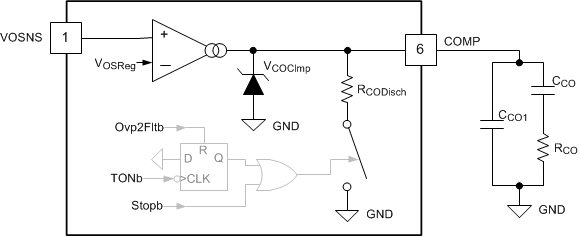
UCC28056 ErrAmpCmp.gifFigure 22. Transconductance Error Amplifier with Typical Compensation Network

To improve the transient response to large perturbations, the error amplifier gain increases by a factor of six times (6×) when the error amplifier input deviates more than ±3% from the nominal regulation voltage, VOSReg. This increase allows faster charging and discharging of the compensation components to recover from step changes in load current.