SLUS456F April   1999  – July 2018 UCC2808A-1 , UCC2808A-2 , UCC3808A-1 , UCC3808A-2

PRODUCTION DATA.  

  1. Features
  2. Applications
  3. Description
    1.     Device Images
      1.      Simplified Application
  4. Revision History
  5. Pin Configuration and Functions
    1.     Pin Functions
  6. Specifications
    1. 6.1 Absolute Maximum Ratings
    2. 6.2 ESD Ratings
    3. 6.3 Recommended Operating Conditions
    4. 6.4 Thermal Information
    5. 6.5 Electrical Characteristics
    6. 6.6 Typical Characteristics
  7. Detailed Description
    1. 7.1 Overview
    2. 7.2 Functional Block Diagrams
    3. 7.3 Feature Description
      1. 7.3.1 Pin Descriptions
        1. 7.3.1.1 COMP
        2. 7.3.1.2 CS
        3. 7.3.1.3 FB
        4. 7.3.1.4 GND
        5. 7.3.1.5 OUTA and OUTB
        6. 7.3.1.6 RC
        7. 7.3.1.7 VDD
    4. 7.4 Device Functional Modes
      1. 7.4.1 VCC
      2. 7.4.2 Push-Pull or Half-Bridge Function
  8. Application and Implementation
    1. 8.1 Application Information
    2. 8.2 Typical Application
      1. 8.2.1 Design Requirements
      2. 8.2.2 Detailed Design Procedure
      3. 8.2.3 Application Curves
  9. Power Supply Recommendations
  10. 10Layout
    1. 10.1 Layout Guidelines
    2. 10.2 Layout Example
  11. 11Device and Documentation Support
    1. 11.1 Documentation Support
      1. 11.1.1 Related Documentation
    2. 11.2 Related Links
    3. 11.3 Receiving Notification of Documentation Updates
    4. 11.4 Community Resources
    5. 11.5 Trademarks
    6. 11.6 Electrostatic Discharge Caution
    7. 11.7 Glossary
  12. 12Mechanical, Packaging, and Orderable Information

Package Options

Refer to the PDF data sheet for device specific package drawings

Mechanical Data (Package|Pins)
  • D|8
  • PW|8
Thermal pad, mechanical data (Package|Pins)
Orderable Information

Functional Block Diagrams

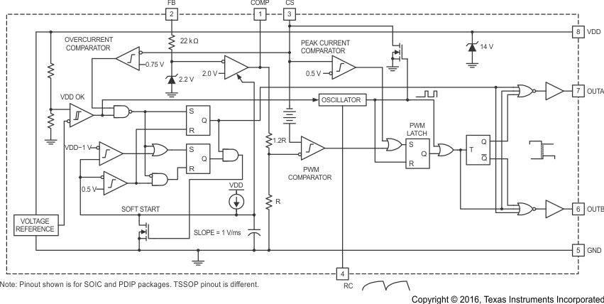
UCC2808A-1 UCC2808A-2 UCC3808A-1 UCC3808A-2 block_diagram_slus456.gif
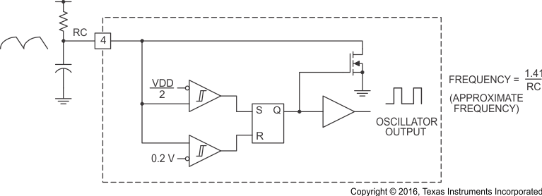
The oscillator generates a sawtooth waveform on RC. During the RC rise time, the output stages alternate on time, but both stages are off during the RC fall time. The output stages switch a 1/2 the oscillator frequency, with ensured duty cycle of < 50% for both outputs.
Figure 9. Block Diagram
UCC2808A-1 UCC2808A-2 UCC3808A-1 UCC3808A-2 block_diagram_oscillator_slus456.gifFigure 10. Block Diagram of Oscillator