SLUS161G April 1999 – April 2025 UCC2813-0 , UCC2813-1 , UCC2813-2 , UCC2813-3 , UCC2813-4 , UCC2813-5 , UCC3813-0 , UCC3813-1 , UCC3813-2 , UCC3813-3 , UCC3813-4 , UCC3813-5
PRODUCTION DATA
- 1
- 1 Features
- 2 Applications
- 3 Description
- 4 Device Comparison Table
- 5 Pin Configuration and Functions
- 6 Specifications
-
7 Detailed Description
- 7.1 Overview
- 7.2 Functional Block Diagram
- 7.3
Feature Description
- 7.3.1 Detailed Pin Descriptions
- 7.3.2 Undervoltage Lockout (UVLO)
- 7.3.3 Self-Biasing, Active Low Output
- 7.3.4 Reference Voltage
- 7.3.5 Oscillator
- 7.3.6 Synchronization
- 7.3.7 PWM Generator
- 7.3.8 Minimum Off-Time Adjustment (Dead-Time Control)
- 7.3.9 Leading Edge Blanking
- 7.3.10 Minimum Pulse Width
- 7.3.11 Current Limiting
- 7.3.12 Overcurrent Protection and Full-Cycle Restart
- 7.3.13 Soft Start
- 7.3.14 Slope Compensation
- 7.4 Device Functional Modes
-
8 Application and Implementation
- 8.1 Application Information
- 8.2
Typical Application
- 8.2.1 Design Requirements
- 8.2.2
Detailed Design Procedure
- 8.2.2.1 Bulk Capacitor Calculation
- 8.2.2.2 Transformer Design
- 8.2.2.3 MOSFET and Output Diode Selection
- 8.2.2.4 Output Capacitor Calculation
- 8.2.2.5 Current Sensing Network
- 8.2.2.6 Gate Drive Resistor
- 8.2.2.7 REF Bypass Capacitor
- 8.2.2.8 RT and CT
- 8.2.2.9 Start-Up Circuit
- 8.2.2.10 Voltage Feedback Compensation Procedure
- 8.2.3 Application Curves
- 8.3 Power Supply Recommendations
- 8.4 Layout
- 9 Device and Documentation Support
- 10Revision History
- 11Mechanical, Packaging, and Orderable Information
Package Options
Refer to the PDF data sheet for device specific package drawings
Mechanical Data (Package|Pins)
- D|8
- PW|8
Thermal pad, mechanical data (Package|Pins)
Orderable Information
7.3.3 Self-Biasing, Active Low Output
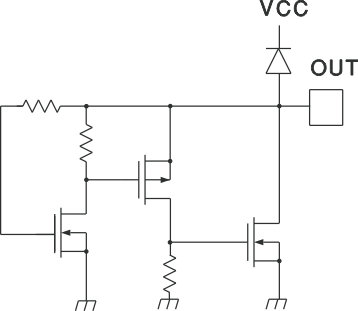
The self-biasing, active-low clamp circuit shown in Figure 7-2 eliminates the potential for problematic MOSFET turnon. As the PWM output voltage rises while in UVLO, the P-channel device drives the larger N-channel switch ON, which clamps the output voltage low. Power to this circuit is supplied by the externally rising gate voltage, so full protection is available regardless of the device's supply voltage during undervoltage lockout.
 Figure 7-2 Internal Circuit Holding OUT Low During UVLO
 Figure 7-3 OUT Voltage vs OUT Current During UVLO