SGLS245E May 2020 – May 2020 UCC2813-0-Q1 , UCC2813-1-Q1 , UCC2813-2-Q1 , UCC2813-3-Q1 , UCC2813-4-Q1 , UCC2813-5-Q1
PRODUCTION DATA.
- 1 Features
- 2 Applications
- 3 Description
- 4 Revision History
- 5 Device Comparison Table
- 6 Pin Configuration and Functions
- 7 Specifications
-
8 Detailed Description
- 8.1 Overview
- 8.2 Functional Block Diagram
- 8.3
Feature Description
- 8.3.1 Detailed Pin Descriptions
- 8.3.2 Undervoltage Lockout (UVLO)
- 8.3.3 Self-Biasing, Active Low Output
- 8.3.4 Reference Voltage
- 8.3.5 Oscillator
- 8.3.6 Synchronization
- 8.3.7 PWM Generator
- 8.3.8 Minimum Off-Time Adjustment (Dead-Time Control)
- 8.3.9 Leading Edge Blanking
- 8.3.10 Minimum Pulse Width
- 8.3.11 Current Limiting
- 8.3.12 Overcurrent Protection and Full-Cycle Restart
- 8.3.13 Soft Start
- 8.3.14 Slope Compensation
- 8.4 Device Functional Modes
-
9 Application and Implementation
- 9.1 Application Information
- 9.2
Typical Application
- 9.2.1 Design Requirements
- 9.2.2
Detailed Design Procedure
- 9.2.2.1 Bulk Capacitor Calculation
- 9.2.2.2 Transformer Design
- 9.2.2.3 MOSFET and Output Diode Selection
- 9.2.2.4 Output Capacitor Calculation
- 9.2.2.5 Current Sensing Network
- 9.2.2.6 Gate Drive Resistor
- 9.2.2.7 REF Bypass Capacitor
- 9.2.2.8 RT and CT
- 9.2.2.9 Start-Up Circuit
- 9.2.2.10 Voltage Feedback Compensation Procedure
- 9.2.3 Application Curves
- 10Power Supply Recommendations
- 11Layout
- 12Device and Documentation Support
- 13Mechanical, Packaging, and Orderable Information
Package Options
Refer to the PDF data sheet for device specific package drawings
Mechanical Data (Package|Pins)
- D|8
Thermal pad, mechanical data (Package|Pins)
Orderable Information
8.3.11 Current Limiting
A 1-V (typical) cycle-by-cycle current limit threshold is incorporated into the UCC2813-x-Q1 family. The 100-ns leading-edge-blanking interval is applied to this current-limiting circuitry. The blanking overrides the current-limit comparator output to prevent the leading-edge switch noise from triggering a current-limit function. Propagation delay from the current-limit comparator to the output is typically 70 ns. This high-speed path minimizes power semiconductor dissipation during an overload by abbreviating the ON time.
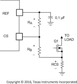
For increased efficiency in the current-sense circuitry, the circuit shown in Figure 26 can be used. Resistors RA and RB bias the actual current-sense resistor voltage up, allowing a smaller current sense amplitude to be used. This circuitry provides current-limiting protection with lower power-loss current sensing.
 Figure 26. Biasing CS For Lower
Current-Sense Voltage
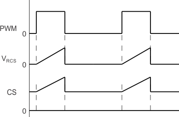
 Figure 27. CS Pin Voltage with Biasing
 The example shown uses a 200-mV full-scale signal at the current sense resistor. Resistor RB biases this up by approximately 700 mV to match the 0.9-V minimum specification of the current-limit comparator of the IC. The value of resistor RA changes with the specific device used, due to the different reference voltages. The resistor values should be selected for minimal power loss. For example, a 50-µA bias current sets RB = 13 kΩ, and RA = 75 kΩ for UCC2813-[0,1,2,4]-Q1 or RA = 56 kΩ for UCC2813-[3,5]-Q1 devices.