SLUSBW3D March 2014 – December 2017 UCC28630 , UCC28631 , UCC28632 , UCC28633 , UCC28634
PRODUCTION DATA.
- 1 Features
- 2 Applications
- 3 Description
- 4 Revision History
- 5 Device Comparison Table
- 6 Pin Configuration and Functions
- 7 Specifications
-
8 Detailed Description
- 8.1 Overview
- 8.2 Functional Block Diagram
- 8.3
Feature Description
- 8.3.1 High-Voltage Current Source Start-Up Operation
- 8.3.2 AC Input UVLO / Brownout Protection
- 8.3.3 Active X-Capacitor Discharge (UCC28630 and UCC28633 only)
- 8.3.4 Magnetic Input and Output Voltage Sensing
- 8.3.5 Fixed-Point Magnetic Sense Sampling Error Sources
- 8.3.6 Magnetic Sense Resistor Network Calculations
- 8.3.7 Magnetic Sensing: Power Stage Design Constraints
- 8.3.8 Magnetic Sense Voltage Control Loop
- 8.3.9 Peak Current Mode Control
- 8.3.10 IPEAK Adjust vs. Line
- 8.3.11 Primary-Side Constant-Current Limit (CC Mode)
- 8.3.12 Primary-Side Overload Timer (UCC28630 only)
- 8.3.13 Overload Timer Adjustment (UCC28630 only)
- 8.3.14 CC-Mode IOUT(lim) Adjustment
- 8.3.15 Fault Protections
- 8.3.16 Pin-Fault Detection and Protection
- 8.3.17 Over-Temperature Protection
- 8.3.18 External Fault Input
- 8.3.19 External SD Pin Wake Input (except UCC28633)
- 8.3.20 External Wake Input at VSENSE Pin (UCC28633 Only)
- 8.3.21 Mode Control and Switching Frequency Modulation
- 8.3.22 Frequency Dither For EMI (except UCC28632)
- 8.4 Device Functional Modes
-
9 Applications and Implementation
- 9.1 Application Information
- 9.2
Typical Application
- 9.2.1 Notebook Adapter, 19.5 V, 65 W
- 9.2.2 UCC28630 Application Schematic
- 9.2.3 Design Requirements
- 9.2.4
Detailed Design Procedure
- 9.2.4.1 Custom Design With WEBENCH® Tools
- 9.2.4.2 Input Bulk Capacitance and Minimum Bulk Voltage
- 9.2.4.3 Transformer Turn Ratio
- 9.2.4.4 Transformer Magnetizing Inductance
- 9.2.4.5 Current Sense Resistor RCS
- 9.2.4.6 Transformer Constraint Verification
- 9.2.4.7 Transformer Selection and Design
- 9.2.4.8 Slope Compensation Verification
- 9.2.4.9 Power MOSFET and Output Rectifier Selection
- 9.2.4.10 Output Capacitor Selection
- 9.2.4.11 Calculation of CC Mode Limit Point
- 9.2.4.12 VDD Capacitor Selection
- 9.2.4.13 Magnetic Sense Resistor Network Selection
- 9.2.4.14 Output LED Pre-Load Resistor Calculation
- 9.2.5 External Wake Pulse Calculation at VSENSE Pin (UCC28633 Only)
- 9.2.6 Energy Star Average Efficiency and Standby Power
- 9.2.7 Application Performance Plots
- 9.3 Dos and Don'ts
- 10Power Supply Recommendations
- 11Layout
- 12Device and Documentation Support
- 13Mechanical, Packaging, and Orderable Information
Package Options
Mechanical Data (Package|Pins)
- D|7
Thermal pad, mechanical data (Package|Pins)
Orderable Information
8.3.2 AC Input UVLO / Brownout Protection
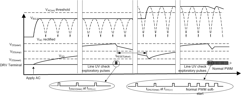
At start-up, once the VDD pin has reached the VDD(start) level, the internal start-up current source is turned off. The controller tests the voltage across the bulk capacitor to determine if the level is high enough to allow the power stage to start, if it has exceeded the rising ACON level. Because there is no load across the bulk capacitor at this stage, the bulk voltage can be used as a proxy for the peak of the AC line. In order to measure the bulk voltage in a low-loss fashion, the controller generates a sequence of three exploratory switching pulses at a frequency of fSW(uv), at minimum peak-current demand level VCS(min) to avoid audible noise, and to deliver minimum energy to the output of the power stage.
Based on the magnetic sampling information determined via the bias winding during these switching pulses, if the output voltage is greater than the output overvoltage threshold, the pulsing stops immediately, and the controller transitions into latched-fault mode. If, however, there is no overvoltage condition detected at the output, the pulse-set completes. If the sensed line voltage is above the line ACON start threshold, then the controller starts up normally, and begins to generate the PWM drive pulses that charge and regulate the output voltage. Alternatively, if the sensed bulk level is below the ACON threshold, then the controller enters low power mode for the reset period (tRESET(short)). It then depletes the VDD rail to the VDD(reset) level. At this point, the start-up sequence repeats, and the device generates another set of exploratory switching pulses. This sequence repeats indefinitely until the AC input is increased to a sufficient level that the bulk voltage exceeds the ACON level.
 Figure 17. AC Input UVLO Detection and Start Up
 Once started, the controller regularly monitors the bulk capacitor voltage. Because the ripple on the bulk capacitor depends on the load level, the device determines the maximum bulk level every 11 ms (approprite for minimum AC frequency of 47 Hz), so the AC peak can be determined. The controller provides input undervoltage protection based on the sensed AC peak level. Once the peak drops below the ACOFF level for the delay period (tUV(delay)), the PWM switching halts, and the controller enters low-power mode for the reset period (tRESET(short)). The device then discharges the bias voltage to the VDD(reset) level, followed by a restart sequence. The controller cycles through the ACON, monitoring (detailed above) indefinitely until the AC input again rises above the ACON level.