SLUSBW3D March 2014 – December 2017 UCC28630 , UCC28631 , UCC28632 , UCC28633 , UCC28634
PRODUCTION DATA.
- 1 Features
- 2 Applications
- 3 Description
- 4 Revision History
- 5 Device Comparison Table
- 6 Pin Configuration and Functions
- 7 Specifications
-
8 Detailed Description
- 8.1 Overview
- 8.2 Functional Block Diagram
- 8.3
Feature Description
- 8.3.1 High-Voltage Current Source Start-Up Operation
- 8.3.2 AC Input UVLO / Brownout Protection
- 8.3.3 Active X-Capacitor Discharge (UCC28630 and UCC28633 only)
- 8.3.4 Magnetic Input and Output Voltage Sensing
- 8.3.5 Fixed-Point Magnetic Sense Sampling Error Sources
- 8.3.6 Magnetic Sense Resistor Network Calculations
- 8.3.7 Magnetic Sensing: Power Stage Design Constraints
- 8.3.8 Magnetic Sense Voltage Control Loop
- 8.3.9 Peak Current Mode Control
- 8.3.10 IPEAK Adjust vs. Line
- 8.3.11 Primary-Side Constant-Current Limit (CC Mode)
- 8.3.12 Primary-Side Overload Timer (UCC28630 only)
- 8.3.13 Overload Timer Adjustment (UCC28630 only)
- 8.3.14 CC-Mode IOUT(lim) Adjustment
- 8.3.15 Fault Protections
- 8.3.16 Pin-Fault Detection and Protection
- 8.3.17 Over-Temperature Protection
- 8.3.18 External Fault Input
- 8.3.19 External SD Pin Wake Input (except UCC28633)
- 8.3.20 External Wake Input at VSENSE Pin (UCC28633 Only)
- 8.3.21 Mode Control and Switching Frequency Modulation
- 8.3.22 Frequency Dither For EMI (except UCC28632)
- 8.4 Device Functional Modes
-
9 Applications and Implementation
- 9.1 Application Information
- 9.2
Typical Application
- 9.2.1 Notebook Adapter, 19.5 V, 65 W
- 9.2.2 UCC28630 Application Schematic
- 9.2.3 Design Requirements
- 9.2.4
Detailed Design Procedure
- 9.2.4.1 Custom Design With WEBENCH® Tools
- 9.2.4.2 Input Bulk Capacitance and Minimum Bulk Voltage
- 9.2.4.3 Transformer Turn Ratio
- 9.2.4.4 Transformer Magnetizing Inductance
- 9.2.4.5 Current Sense Resistor RCS
- 9.2.4.6 Transformer Constraint Verification
- 9.2.4.7 Transformer Selection and Design
- 9.2.4.8 Slope Compensation Verification
- 9.2.4.9 Power MOSFET and Output Rectifier Selection
- 9.2.4.10 Output Capacitor Selection
- 9.2.4.11 Calculation of CC Mode Limit Point
- 9.2.4.12 VDD Capacitor Selection
- 9.2.4.13 Magnetic Sense Resistor Network Selection
- 9.2.4.14 Output LED Pre-Load Resistor Calculation
- 9.2.5 External Wake Pulse Calculation at VSENSE Pin (UCC28633 Only)
- 9.2.6 Energy Star Average Efficiency and Standby Power
- 9.2.7 Application Performance Plots
- 9.3 Dos and Don'ts
- 10Power Supply Recommendations
- 11Layout
- 12Device and Documentation Support
- 13Mechanical, Packaging, and Orderable Information
Package Options
Mechanical Data (Package|Pins)
- D|7
Thermal pad, mechanical data (Package|Pins)
Orderable Information
8.3.5 Fixed-Point Magnetic Sense Sampling Error Sources
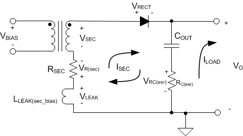
To support operation in CCM, and allow operation at fixed frequency over a large percentage of the load range, the UCC2863x uses fixed-point sampling rather than knee-point detection. When conventionally used, fixed-point sampling typically suffers from poorer regulation performance. This poor performance results from the voltage drops across the secondary-side parasitic resistance RSEC, and the secondary-side leakage inductance from secondary-side to bias LLK(sec_bias), as a consequence of the fact that current remains flowing on the secondary-side when the device measures the output voltage. As shown in Figure 27, the secondary-side pin voltage that gets reflected to the bias winding is detailed in Equation 9.

Equation 9 can be expanded and rearranged into Equation 10.

 Figure 27. Secondary-Side Pin Voltage Contributors with Secondary-Side Current Flow
 Many elements contribute errors to the sensed secondary-side pin voltage, when measured across the bias winding:
- VL(leak): Negative voltage drop across the sec-bias leakage inductance LLK(sec_bias); assuming constant regulated output voltage, this voltage drop is fixed constant offset, because VOUT/LSEC is constant as long as the output is in regulation.
- VRECT: Positive voltage drop across the output rectifier (assuming use of a conventional diode). This voltage drop varies with load current and temperature. However, a constant nominal voltage drop can usually be used, because the increasing forward voltage drop with increasing load current is largely cancelled by the decrease in forward drop as a result of the temperature rise that results.
- VR(sec): This is the drop across the secondary-side winding resistance. This value depends on loading, and varies in proportion to the primary peak current demand that is set by the modulator.
- VRC(esr): This is the drop across the output capacitor equivalent series resistance (esr). This value depends on the difference between the secondary-side winding current and the DC load current being drawn.
Typically, the peak secondary-side winding current ISEC is many times larger than the load current, and the secondary-side winding resistance is typically larger than the output capacitor esr. Thus, the last term in Equation 10 involving ILOAD can typically be neglected.
The leakage inductance and secondary-side rectifier terms represent quasi-constant offset terms, so do not affect regulation to a significant extent. Thus, the quasi-constant offset terms can be accounted for in the calculation of the required scaling resistors to produce the desired setpoint voltage.
The remaining term that dominates the regulation error in Equation 10 is the drop across the secondary-side winding resistance and capacitor esr at the sample instant, {ISEC x(RSEC + RC(esr))}. The controller internally adjusts the control loop reference in proportion to the primary peak current demand in order to null the ISEC related error term in the sampled bias winding voltage. Since the peak secondary-side current ISEC(pk) is the primary peak current IPRI(pk) scaled by the transformer turns ratio, the internal control loop reference effectively varies in approximate proportion to ISEC, resulting in dramatically improved regulation performance.
This improved regulation performance allows the use of primary-side regulation in a wider range of applications, and at unprecedented power levels, operating in both CCM and DCM.