SLUSBW3D March 2014 – December 2017 UCC28630 , UCC28631 , UCC28632 , UCC28633 , UCC28634
PRODUCTION DATA.
- 1 Features
- 2 Applications
- 3 Description
- 4 Revision History
- 5 Device Comparison Table
- 6 Pin Configuration and Functions
- 7 Specifications
-
8 Detailed Description
- 8.1 Overview
- 8.2 Functional Block Diagram
- 8.3
Feature Description
- 8.3.1 High-Voltage Current Source Start-Up Operation
- 8.3.2 AC Input UVLO / Brownout Protection
- 8.3.3 Active X-Capacitor Discharge (UCC28630 and UCC28633 only)
- 8.3.4 Magnetic Input and Output Voltage Sensing
- 8.3.5 Fixed-Point Magnetic Sense Sampling Error Sources
- 8.3.6 Magnetic Sense Resistor Network Calculations
- 8.3.7 Magnetic Sensing: Power Stage Design Constraints
- 8.3.8 Magnetic Sense Voltage Control Loop
- 8.3.9 Peak Current Mode Control
- 8.3.10 IPEAK Adjust vs. Line
- 8.3.11 Primary-Side Constant-Current Limit (CC Mode)
- 8.3.12 Primary-Side Overload Timer (UCC28630 only)
- 8.3.13 Overload Timer Adjustment (UCC28630 only)
- 8.3.14 CC-Mode IOUT(lim) Adjustment
- 8.3.15 Fault Protections
- 8.3.16 Pin-Fault Detection and Protection
- 8.3.17 Over-Temperature Protection
- 8.3.18 External Fault Input
- 8.3.19 External SD Pin Wake Input (except UCC28633)
- 8.3.20 External Wake Input at VSENSE Pin (UCC28633 Only)
- 8.3.21 Mode Control and Switching Frequency Modulation
- 8.3.22 Frequency Dither For EMI (except UCC28632)
- 8.4 Device Functional Modes
-
9 Applications and Implementation
- 9.1 Application Information
- 9.2
Typical Application
- 9.2.1 Notebook Adapter, 19.5 V, 65 W
- 9.2.2 UCC28630 Application Schematic
- 9.2.3 Design Requirements
- 9.2.4
Detailed Design Procedure
- 9.2.4.1 Custom Design With WEBENCH® Tools
- 9.2.4.2 Input Bulk Capacitance and Minimum Bulk Voltage
- 9.2.4.3 Transformer Turn Ratio
- 9.2.4.4 Transformer Magnetizing Inductance
- 9.2.4.5 Current Sense Resistor RCS
- 9.2.4.6 Transformer Constraint Verification
- 9.2.4.7 Transformer Selection and Design
- 9.2.4.8 Slope Compensation Verification
- 9.2.4.9 Power MOSFET and Output Rectifier Selection
- 9.2.4.10 Output Capacitor Selection
- 9.2.4.11 Calculation of CC Mode Limit Point
- 9.2.4.12 VDD Capacitor Selection
- 9.2.4.13 Magnetic Sense Resistor Network Selection
- 9.2.4.14 Output LED Pre-Load Resistor Calculation
- 9.2.5 External Wake Pulse Calculation at VSENSE Pin (UCC28633 Only)
- 9.2.6 Energy Star Average Efficiency and Standby Power
- 9.2.7 Application Performance Plots
- 9.3 Dos and Don'ts
- 10Power Supply Recommendations
- 11Layout
- 12Device and Documentation Support
- 13Mechanical, Packaging, and Orderable Information
Package Options
Mechanical Data (Package|Pins)
- D|7
Thermal pad, mechanical data (Package|Pins)
Orderable Information
8.3.20 External Wake Input at VSENSE Pin (UCC28633 Only)
The UCC28633 device variant supports fast PSR transient response via the VSENSE pin. When the loop demand drives the modulator frequency below approximately fSMP(max), the controller enters a low-power sleep mode for a portion of the switching cycle. The sleep interval varies, depending on the switching frequency commanded. The sleep interval is longer for lower switching frequency, and longest at fSW(min). For conventional PSR controllers, if a load transient occurs during this sleep interval, the controller will not react until the next timed wake-up, during which the output voltage can drop significantly, depending on the size of the load step and the amount of output capacitance.
The UCC28633 can respond to fast transient wake signal coupled to the VSENSE pin. If the wake signal exceeds an internal pin threshold VSENSE(wake) while the controller is in sleep mode, the sleep interval is terminated and PWM activity commences within a typical delay time of tWAKE. This dramatically improves the response to heavy load transients from zero load, or very light load. If the switching frequency is above fSMP(max), the controller never enters sleep mode, so wake response on the VSENSE pin never enabled. The commencement of any sleep interval in the controller is delayed until the resonant ringing on the VENSE pin has decreased below the VSENSE(wake) threshold for at least 2 µs. Once the ringing has decreased, the wake response is enabled, and the sleep interval commences.
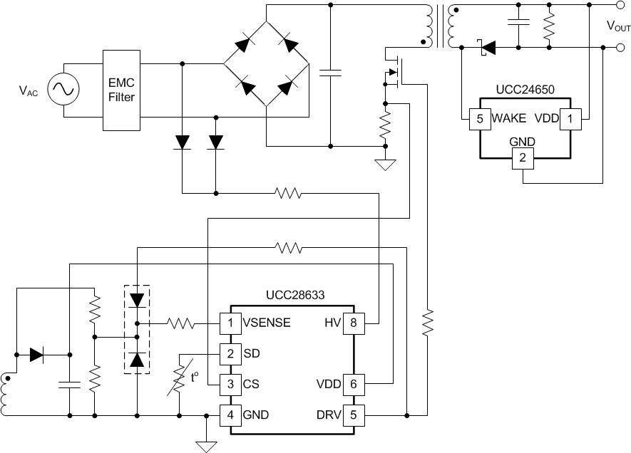
 Figure 39. UCC24650 Secondary-Side Voltage Monitor and Wake-Up Circuit
 The wake signal at the VSENSE pin can be generated using a secondary side low power voltage monitor such as UCC24650, as shown in Figure 39. Further details can be found in the datasheet for UCC24650. This secondary-side monitor uses the switching activity on the secondary winding to trigger refresh of an internal sample-and-hold circuit to measure and record the system output voltage at the VDD pin. Thereafter, if the actual output voltage, sensed at the VDD pin, drops by ΔWAKE% (see UCC24650 detailed datasheet specifications) of the previously sampled value, the WAKE pin is internally pulled low through a current-limited open-drain switch. As shown in Figure 39, the main output rectifier diode is positioned at the return side of the secondary winding, so that the GND-referenced UCC24650 WAKE function can be deployed. In effect, the WAKE pin shorts out the rectifier diode for a short interval (see UCC24650 detailed datasheet specifications), to draw some current from the output capacitor through the transformer secondary winding. This sets up a low-level pulse of current that then rings resonantly in the power circuit magnetizing inductance and parasitic capacitance. The ringing causes a similar ringing voltage waveform on all transformer windings, including the bias/sense winding, which interfaces to the VSENSE pin. If the initial pulse of current drawn by the secondary WAKE pin is sufficient, then the ringing voltage at the VSENSE pin is large enough to exceed the VSENSE(wake) threshold.
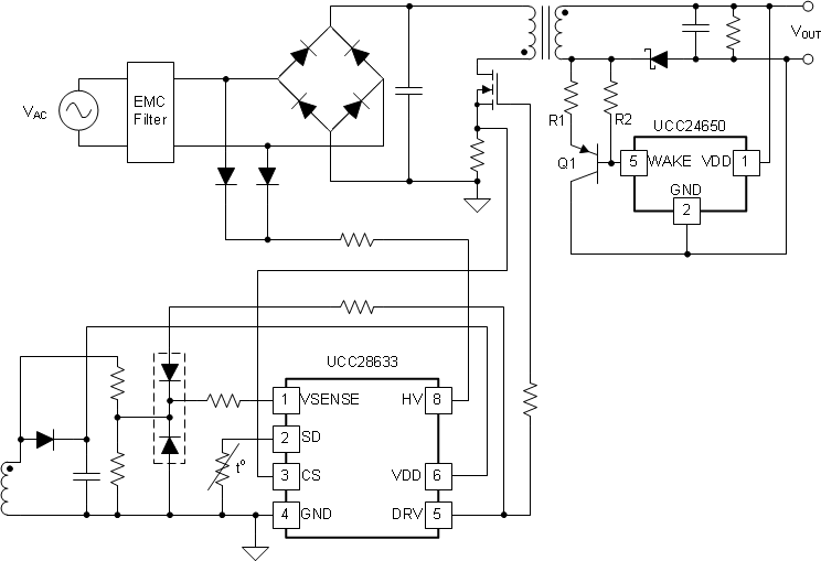
The UCC24650 datasheet Application Information section includes details of how to estimate the amplitude of the wake-pulse ringing at the WAKE pin. In some cases, especially at higher rated output power, the transformer magnetizing inductance is lower, while the total switch node capacitance tends to be higher. This reduces the transformer impedance, and can also result in reduced wake pulse amplitude. In these cases, the UCC24650 WAKE pin output can be augmented with an external PNP circuit Q1, R1 and R2, as shown in Figure 40. In this case, when the WAKE pin pulls low, Q1 turns on, and draws more current through the secondary winding. A current limiting resistor R1 is recommended in series with either collector or emitter. Effectively R1 swamps the UCC24650 internal WAKE pin resistance, RWAKE. A pull-up resistor R2 from base to emitter is also required, to ensure that the WAKE pin is adequately pulled up/down during normal switching activity to properly trigger the internal sample and hold on the VDD pin. The external PNP device Q1 must have at least the same voltage rating as the main rectifier diode.
