SLUSCA8A February 2016 – February 2016 UCC28704
PRODUCTION DATA.
- 1 Features
- 2 Applications
- 3 Description
- 4 Revision History
- 5 Pin Configuration and Functions
- 6 Specifications
-
7 Detailed Description
- 7.1 Overview
- 7.2 Functional Block Diagram
- 7.3
Feature Description
- 7.3.1 Detailed Pin Description
- 7.3.2 Primary-Side Regulation (PSR)
- 7.3.3 Primary-Side Constant Voltage (CV) Regulation
- 7.3.4 Primary-Side Constant Current (CC) Regulation
- 7.3.5 Valley-Switching and Valley-Skipping
- 7.3.6 Start-Up Operation
- 7.3.7 Fault Protection
- 7.3.8 Constant Current Under-Voltage Protection
- 7.3.9 Load Transient Response
- 7.4 Device Functional Modes
-
8 Applications and Implementation
- 8.1 Application Information
- 8.2
Typical Application
- 8.2.1 Design Requirements
- 8.2.2
Detailed Design Procedure
- 8.2.2.1 VDD Capacitance, CDD
- 8.2.2.2 VDD Start-Up Resistance, RSTR
- 8.2.2.3 Input Bulk Capacitance and Minimum Bulk Voltage
- 8.2.2.4 Transformer Turns Ratio, Inductance, Primary-Peak Current
- 8.2.2.5 Transformer Parameter Verification
- 8.2.2.6 VS Resistor Divider, Line Compensation, and NTC
- 8.2.2.7 Standby Power Estimate
- 8.2.2.8 Output Capacitance
- 8.2.2.9 Design Considerations in Using with Synchronous Rectifiers
- 8.2.3 Application Curves
- 8.3 Do's and Don'ts
- 9 Power Supply Recommendations
- 10Layout
-
11Device and Documentation Support
- 11.1
Device Support
- 11.1.1
Device Nomenclature
- 11.1.1.1 Capacitance Terms in Farads
- 11.1.1.2 Duty Cycle Terms
- 11.1.1.3 Frequency Terms in Hertz
- 11.1.1.4 Current Terms in Amperes
- 11.1.1.5 Current and Voltage Scaling Terms
- 11.1.1.6 Transformer Terms
- 11.1.1.7 Power Terms in Watts
- 11.1.1.8 Resistance Terms in Ω
- 11.1.1.9 Timing Terms in Seconds
- 11.1.1.10 Voltage Terms in Volts
- 11.1.1.11 AC Voltage Terms in VRMS
- 11.1.1.12 Efficiency Terms
- 11.1.1
Device Nomenclature
- 11.2 Documentation Support
- 11.3 Community Resources
- 11.4 Trademarks
- 11.5 Electrostatic Discharge Caution
- 11.6 Glossary
- 11.1
Device Support
- 12Mechanical, Packaging, and Orderable Information
Package Options
Mechanical Data (Package|Pins)
- DBV|6
Thermal pad, mechanical data (Package|Pins)
Orderable Information
1 Features
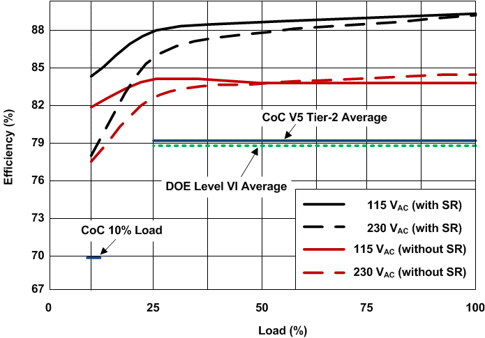
- Efficiency Performance Exceeds DoE Level VI and EU CoC V5 Tier-2 External Power Supply Standards
- Primary-Side Regulation Eliminates Opto-Coupler and Secondary Feedback Components
- Compatible with Synchronous Rectifier
- Enables <30-mW No-Load Input Power
- ±5% Output Voltage (CV) and Current (CC) Regulation
- Enhanced Dynamic Load Response
- Constant Current Output Under-Voltage Protection (CCUV) with Auto-Restart Response
- Cable Compensation (300 mV at 5-V Full Load)
- 85-kHz Maximum Switching Frequency
- DCM Valley-Switching Operation
- Clamped Gate-Drive Output for MOSFET
- NTC Resistor Interface
- Resistor or External HV Depletion-Mode FET Start-Up
- Fault Protections: Input Low Line, Output Over-Voltage, Over-Current, and Short-Circuit
- SOT23-6 Package
2 Applications
- Adapters and Chargers for Phones and Tablets
- USB Type-C AC Adapters for Consumer Electronics
- Low Power AC to DC SMPS
- Industrial and Medical SMPS
3 Description
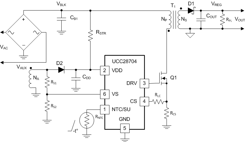
The UCC28704 Off-line flyback controller is a highly integrated, 6-pin primary-side regulated PWM controller for designing high efficiency AC-to-DC power supplies with low standby power consumption to comply with global efficiency standards. The controller has ultra-low current consumption at start-up to enable designs with <30-mW no-load input power and save standby mode energy consumption. Intelligent primary-side sensing and control enables 5% output voltage and current control without using an opto coupler or secondary-side feedback circuits.
UCC28704 incorporates an enhanced load transient response technique which helps minimize the output capacitor, reducing the overall system size and cost. The controller also eliminates the need for loop compensation components which simplify the design and debugging process for power supply designers. The converter output voltage and current is regulated to prevent overstress conditions that may damage the load or connectors. Similarly, the CCUV shutdown feature monitors for an output under voltage fault to protect connectors from over heat or burn out from soft shorts, which greatly enhance overall system reliability. Board or component over temperature protection is facilitated with an NTC interface pin.
UCC28704 can be readily used with TI secondary-side synchronous rectifier (SR) controllers at 2-A or higher output current levels for higher conversion efficiency or more compact designs.
Device Information (1)
| PART NUMBER | PACKAGE | BODY SIZE (NOM) |
|---|---|---|
| UCC28704 | SOT23-6 | 2.90 mm × 1.60 mm |
- For all available packages, see the orderable addendum at the end of the datasheet.
Simplified Schematic

5-V, 2-A Adapter Efficiency Performance
