SLUSCR9B June 2017 – December 2020 UCC28730-Q1
PRODUCTION DATA
- 1 Features
- 2 Applications
- 3 Description
- 4 Revision History
- 5 Pin Configuration and Functions
- 6 Specifications
-
7 Detailed Description
- 7.1 Overview
- 7.2 Functional Block Diagram
- 7.3 Feature Description
- 7.4 Device Functional Modes
-
8 Application and Implementation
- 8.1 Application Information
- 8.2
Typical Application
- 8.2.1 Design Requirements
- 8.2.2
Detailed Design Procedure
- 8.2.2.1 Stand-By Power Estimate
- 8.2.2.2 Input Bulk Capacitance and Minimum Bulk Voltage
- 8.2.2.3 Transformer Turns Ratio, Inductance, Primary-Peak Current
- 8.2.2.4 Transformer Parameter Verification
- 8.2.2.5 Output Capacitance
- 8.2.2.6 VDD Capacitance, CVDD
- 8.2.2.7 VS Resistor Divider, Line Compensation, and Cable Compensation
- 8.2.2.8 VS Wake-Up Detection
- 8.2.3 Application Curves
- 8.3 Do's and Don'ts
- 9 Power Supply Recommendations
- 10Layout
-
11Device and Documentation Support
- 11.1
Device Support
- 11.1.1
Device Nomenclature
- 11.1.1.1 Capacitance Terms in Farads
- 11.1.1.2 Duty-Cycle Terms
- 11.1.1.3 Frequency Terms in Hertz
- 11.1.1.4 Current Terms in Amperes
- 11.1.1.5 Current and Voltage Scaling Terms
- 11.1.1.6 Transformer Terms
- 11.1.1.7 Power Terms in Watts
- 11.1.1.8 Resistance Terms in Ω
- 11.1.1.9 Timing Terms in Seconds
- 11.1.1.10 DC Voltage Terms in Volts
- 11.1.1.11 AC Voltage Terms in Volts
- 11.1.1.12 Efficiency Terms
- 11.1.1
Device Nomenclature
- 11.2 Documentation Support
- 11.3 Receiving Notification of Documentation Updates
- 11.4 Support Resources
- 11.5 Trademarks
- 11.6 Electrostatic Discharge Caution
- 11.7 Glossary
- 11.1
Device Support
- 12Mechanical, Packaging, and Orderable Information
Package Options
Mechanical Data (Package|Pins)
- D|7
Thermal pad, mechanical data (Package|Pins)
Orderable Information
8.2.2.8 VS Wake-Up Detection
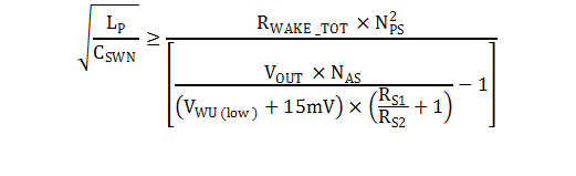
The amplitude of the wake-up signal at the VS input must be high enough to be detected. This signal, which originates on the secondary winding, is limited by the impedances of the wake-up signal driver and the L-C resonant tank of the transformer windings. The signal is further attenuated by the VS divider resistors. To maximize the wake-up signal amplitude, the pulse width, tWAKE, of the wake-up signal should be at least 1/4-wavelength of the switched-node resonant frequency, fRES. The resonant frequency depends on the primary magnetizing inductance and the total equivalent capacitance at the switching node, that is, the primary-side MOSFET drain node. The switched-node capacitance, CSWN, includes the MOSFET COSS, the transformer winding capacitance, and all other stray circuit capacitance attached to the MOSFET drain. Use Equation 31 to determine fRES. Conversely, if fRES is known by experience or measurement, CSWN can be derived from Equation 31.

Since the wake-up pulse width is typically fixed by the driver device, such as the UCC24650, maximum signal strength is obtained when Equation 32 is true. Since LP is generally fixed by other system requirements, only CSWN can be reduced to increase fRES, if necessary.

Equation 33 is used to ensure that there is sufficient amplitude at the VS input to reliably trigger the wake-up function, where RWAKE_TOT is the total secondary-side resistance of the wake-up signal driver and any series resistance. An over-drive of 15 mV is added to the wake-up threshold level for margin.