SLUSCR9B June 2017 – December 2020 UCC28730-Q1
PRODUCTION DATA
- 1 Features
- 2 Applications
- 3 Description
- 4 Revision History
- 5 Pin Configuration and Functions
- 6 Specifications
-
7 Detailed Description
- 7.1 Overview
- 7.2 Functional Block Diagram
- 7.3 Feature Description
- 7.4 Device Functional Modes
-
8 Application and Implementation
- 8.1 Application Information
- 8.2
Typical Application
- 8.2.1 Design Requirements
- 8.2.2
Detailed Design Procedure
- 8.2.2.1 Stand-By Power Estimate
- 8.2.2.2 Input Bulk Capacitance and Minimum Bulk Voltage
- 8.2.2.3 Transformer Turns Ratio, Inductance, Primary-Peak Current
- 8.2.2.4 Transformer Parameter Verification
- 8.2.2.5 Output Capacitance
- 8.2.2.6 VDD Capacitance, CVDD
- 8.2.2.7 VS Resistor Divider, Line Compensation, and Cable Compensation
- 8.2.2.8 VS Wake-Up Detection
- 8.2.3 Application Curves
- 8.3 Do's and Don'ts
- 9 Power Supply Recommendations
- 10Layout
-
11Device and Documentation Support
- 11.1
Device Support
- 11.1.1
Device Nomenclature
- 11.1.1.1 Capacitance Terms in Farads
- 11.1.1.2 Duty-Cycle Terms
- 11.1.1.3 Frequency Terms in Hertz
- 11.1.1.4 Current Terms in Amperes
- 11.1.1.5 Current and Voltage Scaling Terms
- 11.1.1.6 Transformer Terms
- 11.1.1.7 Power Terms in Watts
- 11.1.1.8 Resistance Terms in Ω
- 11.1.1.9 Timing Terms in Seconds
- 11.1.1.10 DC Voltage Terms in Volts
- 11.1.1.11 AC Voltage Terms in Volts
- 11.1.1.12 Efficiency Terms
- 11.1.1
Device Nomenclature
- 11.2 Documentation Support
- 11.3 Receiving Notification of Documentation Updates
- 11.4 Support Resources
- 11.5 Trademarks
- 11.6 Electrostatic Discharge Caution
- 11.7 Glossary
- 11.1
Device Support
- 12Mechanical, Packaging, and Orderable Information
Package Options
Mechanical Data (Package|Pins)
- D|7
Thermal pad, mechanical data (Package|Pins)
Orderable Information
7.3.2 Primary-Side Regulation (PSR)
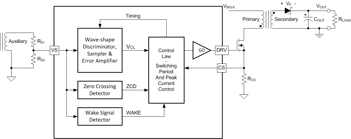
Figure 7-1 illustrates a simplified isolated-flyback convertor with the main voltage regulation blocks of the device shown. The power train operation is the same as any DCM flyback circuit but accurate output voltage and current sensing is the key to primary-side control. The output voltage is sensed as a reflected voltage during the transformer demagnetization time using a divider network at the VS input. The primary winding current is sensed at the CS input using a current-sense resistor, RCS.
 Figure 7-1 Simplified Flyback Convertor (with the main voltage regulation blocks)
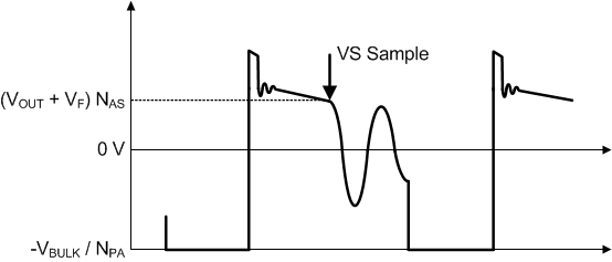
In primary-side control, the output voltage is indirectly sensed on the auxiliary winding at the end of the transfer of stored transformer energy to the secondary. As shown in Figure 7-2 it is clear there is a down slope representing a decreasing total rectifier VF and resistance voltage drop as the secondary current decreases to zero. To achieve an accurate representation of the secondary output voltage on the auxiliary winding, the discriminator reliably blocks the leakage inductance reset and ringing, continuously samples the auxiliary voltage during the down slope after the ringing is diminished, and captures the error signal at the time the secondary winding reaches zero current. The internal reference on VS is 4.04 V. Temperature compensation on the VS reference voltage of -1 mV/°C offsets the change in the forward voltage of the output rectifier with temperature. The resistor divider is selected as outlined in the VS pin description.
 Figure 7-2 Auxiliary Winding Voltage
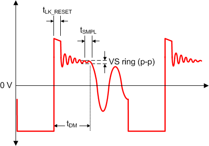
The UCC28730-Q1 VS-signal sampler includes signal discrimination methods to ensure an accurate sample of the output voltage from the auxiliary winding. There are, however, some details of the auxiliary winding signal which require attention to ensure reliable operation, specifically the reset time of the leakage inductance and the duration of any subsequent leakage inductance ring. Refer to Figure 7-3 below for a detailed illustration of waveform criteria to ensure a reliable sample on the VS pin.
 Figure 7-3 Auxiliary Waveform Details
The first detail to examine is the duration of the leakage inductance reset pedestal, tLK_RESET in Figure 7-3. Since this can mimic the waveform of the secondary current decay, followed by a sharp downslope, it is important to keep the leakage reset time to less than 750 ns for IPRI minimum, and to less than 2.25 µs for IPRI maximum.
The second detail is the amplitude of ringing on the VAUX waveform following tLK_RESET. The peak-to-peak voltage at the VS pin should be less than 125 mV for at least 200 ns before the end of the demagnetization time, tDM. If there is a concern with excessive ringing, it usually occurs during light-load or no-load conditions, when tDM is at the minimum. To avoid distorting the signal waveform at VS with oscilloscope probe capacitance, it is recommended to probe the auxiliary winding to view the VS waveform characteristics. The tolerable ripple on VS is scaled up to the auxiliary-winding voltage by RS1 and RS2, and is equal to 125 mV x (RS1 + RS2) / RS2.