SLUSBL5A February 2015 – June 2019 UCC28730
PRODUCTION DATA.
- 1 Features
- 2 Applications
- 3 Description
- 4 Revision History
- 5 Pin Configuration and Functions
- 6 Specifications
-
7 Detailed Description
- 7.1 Overview
- 7.2 Functional Block Diagram
- 7.3 Feature Description
- 7.4 Device Functional Modes
-
8 Application and Implementation
- 8.1 Application Information
- 8.2
Typical Application
- 8.2.1 Design Requirements
- 8.2.2
Detailed Design Procedure
- 8.2.2.1 Stand-By Power Estimate
- 8.2.2.2 Input Bulk Capacitance and Minimum Bulk Voltage
- 8.2.2.3 Transformer Turns Ratio, Inductance, Primary-Peak Current
- 8.2.2.4 Transformer Parameter Verification
- 8.2.2.5 Output Capacitance
- 8.2.2.6 VDD Capacitance, CVDD
- 8.2.2.7 VS Resistor Divider, Line Compensation, and Cable Compensation
- 8.2.2.8 VS Wake-Up Detection
- 8.2.3 Application Curves
- 8.3 Do's and Don'ts
- 9 Power Supply Recommendations
- 10Layout
-
11Device and Documentation Support
- 11.1
Device Support
- 11.1.1 Development Support
- 11.1.2
Device Nomenclature
- 11.1.2.1 Capacitance Terms in Farads
- 11.1.2.2 Duty-Cycle Terms
- 11.1.2.3 Frequency Terms in Hertz
- 11.1.2.4 Current Terms in Amperes
- 11.1.2.5 Current and Voltage Scaling Terms
- 11.1.2.6 Transformer Terms
- 11.1.2.7 Power Terms in Watts
- 11.1.2.8 Resistance Terms in Ω
- 11.1.2.9 Timing Terms in Seconds
- 11.1.2.10 DC Voltage Terms in Volts
- 11.1.2.11 AC Voltage Terms in Volts
- 11.1.2.12 Efficiency Terms
- 11.2 Documentation Support
- 11.3 Receiving Notification of Documentation Updates
- 11.4 Community Resources
- 11.5 Trademarks
- 11.6 Electrostatic Discharge Caution
- 11.7 Glossary
- 11.1
Device Support
- 12Mechanical, Packaging, and Orderable Information
Package Options
Mechanical Data (Package|Pins)
- D|7
Thermal pad, mechanical data (Package|Pins)
Orderable Information
7.3.3 Primary-Side Constant Voltage Regulation
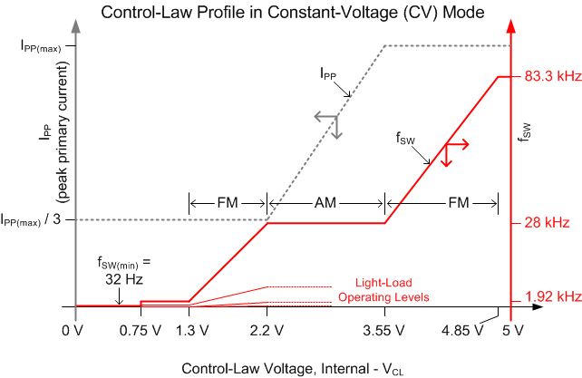
During voltage regulation, the controller operates in frequency modulation and amplitude modulation modes according to the control law as illustrated in Figure 16 below. The control law voltage VCL reflects the internal operating level based on the voltage-error amplifier output signal. Neither of these signals is accessible to the user, however the approximate VCL may be inferred from the frequency and amplitude of the current sense signal at the CS input. As the line and load conditions vary, VCL adjusts the operating frequency and amplitude as required to maintain regulation of the output voltage. Because the UCC28730 incorporates internal loop compensation, no external stability compensation is required.
The internal operating frequency limits of the device are fSW(max) and fSW(min), typically 83.3 kHz and 32 Hz, respectively. The choice of transformer primary inductance and primary-peak current sets the maximum operating frequency of the converter, which must be equal to or lower than fSW(max). Conversely, the choice of maximum target operating frequency and primary-peak current determines the transformer primary-inductance value. The actual minimum switching frequency for any particular converter depends on several factors, including minimum loading level, leakage inductance losses, switched-node capacitance losses, other switching and conduction losses, and bias-supply requirements. In any case, the minimum steady-state frequency of the converter must always exceed fSW(min) or the output voltage may rise to the overvoltage protection level (OVP) and the controller responds as described in the Fault Protection Section.
The steady-state Control-Law voltage, VCL, ranges between 1.3 to 4.85 V, depending on load, but may occasionally move below 0.75 V or above 4.85 V on load transients. Dropping below 0.75 V shifts the switching frequency to a lower range at light loads, while exceeding 4.85 V enters the constant-current mode of operation. There are 3 lower operating frequency ranges for progressively lighter loads, each overlapping the previous range to some extent, to provide stable regulation at very low frequencies. Peak-primary current is always maintained at IPP(max)/3 in these lower frequency levels. Transitions between levels is automatically accomplished by the controller depending on the internal control-law voltage, VCL.
 Figure 16. Frequency and Amplitude Modulation Modes (during voltage regulation)