SLUSBL5A February 2015 – June 2019 UCC28730
PRODUCTION DATA.
- 1 Features
- 2 Applications
- 3 Description
- 4 Revision History
- 5 Pin Configuration and Functions
- 6 Specifications
-
7 Detailed Description
- 7.1 Overview
- 7.2 Functional Block Diagram
- 7.3 Feature Description
- 7.4 Device Functional Modes
-
8 Application and Implementation
- 8.1 Application Information
- 8.2
Typical Application
- 8.2.1 Design Requirements
- 8.2.2
Detailed Design Procedure
- 8.2.2.1 Stand-By Power Estimate
- 8.2.2.2 Input Bulk Capacitance and Minimum Bulk Voltage
- 8.2.2.3 Transformer Turns Ratio, Inductance, Primary-Peak Current
- 8.2.2.4 Transformer Parameter Verification
- 8.2.2.5 Output Capacitance
- 8.2.2.6 VDD Capacitance, CVDD
- 8.2.2.7 VS Resistor Divider, Line Compensation, and Cable Compensation
- 8.2.2.8 VS Wake-Up Detection
- 8.2.3 Application Curves
- 8.3 Do's and Don'ts
- 9 Power Supply Recommendations
- 10Layout
-
11Device and Documentation Support
- 11.1
Device Support
- 11.1.1 Development Support
- 11.1.2
Device Nomenclature
- 11.1.2.1 Capacitance Terms in Farads
- 11.1.2.2 Duty-Cycle Terms
- 11.1.2.3 Frequency Terms in Hertz
- 11.1.2.4 Current Terms in Amperes
- 11.1.2.5 Current and Voltage Scaling Terms
- 11.1.2.6 Transformer Terms
- 11.1.2.7 Power Terms in Watts
- 11.1.2.8 Resistance Terms in Ω
- 11.1.2.9 Timing Terms in Seconds
- 11.1.2.10 DC Voltage Terms in Volts
- 11.1.2.11 AC Voltage Terms in Volts
- 11.1.2.12 Efficiency Terms
- 11.2 Documentation Support
- 11.3 Receiving Notification of Documentation Updates
- 11.4 Community Resources
- 11.5 Trademarks
- 11.6 Electrostatic Discharge Caution
- 11.7 Glossary
- 11.1
Device Support
- 12Mechanical, Packaging, and Orderable Information
Package Options
Mechanical Data (Package|Pins)
- D|7
Thermal pad, mechanical data (Package|Pins)
Orderable Information
8.2 Typical Application
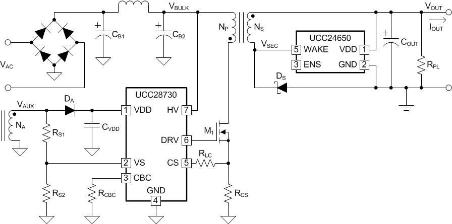
A typical application for the UCC28730 includes the compatible UCC24650 Wake-Up Monitor device to regulate an isolated low-voltage DC output with low output capacitance. When the UCC28730 is operating in the low-frequency Wait state, the UCC24650 alerts the UCC28730 to a sudden load increase, avoiding the need for extremely high output capacitance to hold up between power cycles. As shown in Figure 23, the output rectification uses a ground-referenced diode to facilitate application of the UCC24650. A ground-referenced synchronous rectifier may also be used.
NOTE
Figure 23 is simplified to illustrate the basic application of the UCC28730 and does not show all of the components and networks needed for an actual converter design, nor all of the possible circuit variations.
 Figure 23. Simplified Application With Ground-Referenced Diode