SLUSDT2C August 2019 – December 2020 UCC28740-Q1
PRODUCTION DATA
- 1 Features
- 2 Applications
- 3 Description
- 4 Revision History
- 5 Pin Configuration and Functions
- 6 Specifications
- 7 Detailed Description
-
8 Application and Implementation
- 8.1 Application Information
- 8.2 High Voltage Applications
- 8.3
Typical Application
- 8.3.1 Design Requirements
- 8.3.2
Detailed Design Procedure
- 8.3.2.1 Custom Design With WEBENCH® Tools
- 8.3.2.2 Standby Power Estimate and No-Load Switching Frequency
- 8.3.2.3 Input Bulk Capacitance and Minimum Bulk Voltage
- 8.3.2.4 35
- 8.3.2.5 Transformer Turns-Ratio, Inductance, Primary Peak Current
- 8.3.2.6 Transformer Parameter Verification
- 8.3.2.7 VS Resistor Divider, Line Compensation
- 8.3.2.8 Output Capacitance
- 8.3.2.9 VDD Capacitance, CVDD
- 8.3.2.10 Feedback Network Biasing
- 8.3.3 Application Curves
- 9 Power Supply Recommendations
- 10Layout
-
11Device and Documentation Support
- 11.1
Device Support
- 11.1.1 Development Support
- 11.1.2
Device Nomenclature
- 11.1.2.1 Capacitance Terms in Farads
- 11.1.2.2 Duty Cycle Terms
- 11.1.2.3 Frequency Terms in Hertz
- 11.1.2.4 Current Terms in Amperes
- 11.1.2.5 Current and Voltage Scaling Terms
- 11.1.2.6 Transformer Terms
- 11.1.2.7 Power Terms in Watts
- 11.1.2.8 Resistance Terms in Ohms
- 11.1.2.9 Timing Terms in Seconds
- 11.1.2.10 Voltage Terms in Volts
- 11.1.2.11 AC Voltage Terms in VRMS
- 11.1.2.12 Efficiency Terms
- 11.2 Documentation Support
- 11.3 Receiving Notification of Documentation Updates
- 11.4 Community Resources
- 11.5 Trademarks
- 11.1
Device Support
Package Options
Mechanical Data (Package|Pins)
- D|7
Thermal pad, mechanical data (Package|Pins)
Orderable Information
3 Description
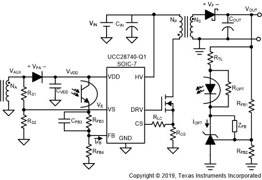
The UCC28740-Q1 isolated-flyback power-supply controller regulates the output using an optical coupler to provide fast transient response to large-load steps.
An internal 700-V startup switch, dynamically controlled operating states, and a tailored modulation profile support ultra-low standby power without sacrificing startup time or output transient response.
Control algorithms in the UCC28740-Q1 allow operating efficiencies to meet or exceed applicable standards. The drive output interfaces to a MOSFET power switch. Discontinuous conduction mode (DCM) with valley-switching reduces switching losses. Modulation of switching frequency and primary current-peak amplitude (FM and AM) keeps the conversion efficiency high across the entire load and line ranges.
The controller has a maximum switching frequency of 100 kHz and always maintains control of the peak-primary current in the transformer. Protection features keep primary and secondary component stresses in check. A minimum switching frequency of 170 Hz facilitates the achievement of less than 10-mW no-load power.
| PART NUMBER | PACKAGE | BODY SIZE (NOM) |
|---|---|---|
| UCC28740-Q1 | SOIC (7) | 4.90 mm × 3.91 mm |
 Simplified Application Diagram
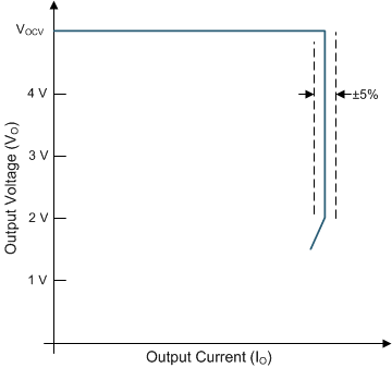
 Typical V-I Diagram