SLUSDT2C August 2019 – December 2020 UCC28740-Q1
PRODUCTION DATA
- 1 Features
- 2 Applications
- 3 Description
- 4 Revision History
- 5 Pin Configuration and Functions
- 6 Specifications
- 7 Detailed Description
-
8 Application and Implementation
- 8.1 Application Information
- 8.2 High Voltage Applications
- 8.3
Typical Application
- 8.3.1 Design Requirements
- 8.3.2
Detailed Design Procedure
- 8.3.2.1 Custom Design With WEBENCH® Tools
- 8.3.2.2 Standby Power Estimate and No-Load Switching Frequency
- 8.3.2.3 Input Bulk Capacitance and Minimum Bulk Voltage
- 8.3.2.4 35
- 8.3.2.5 Transformer Turns-Ratio, Inductance, Primary Peak Current
- 8.3.2.6 Transformer Parameter Verification
- 8.3.2.7 VS Resistor Divider, Line Compensation
- 8.3.2.8 Output Capacitance
- 8.3.2.9 VDD Capacitance, CVDD
- 8.3.2.10 Feedback Network Biasing
- 8.3.3 Application Curves
- 9 Power Supply Recommendations
- 10Layout
-
11Device and Documentation Support
- 11.1
Device Support
- 11.1.1 Development Support
- 11.1.2
Device Nomenclature
- 11.1.2.1 Capacitance Terms in Farads
- 11.1.2.2 Duty Cycle Terms
- 11.1.2.3 Frequency Terms in Hertz
- 11.1.2.4 Current Terms in Amperes
- 11.1.2.5 Current and Voltage Scaling Terms
- 11.1.2.6 Transformer Terms
- 11.1.2.7 Power Terms in Watts
- 11.1.2.8 Resistance Terms in Ohms
- 11.1.2.9 Timing Terms in Seconds
- 11.1.2.10 Voltage Terms in Volts
- 11.1.2.11 AC Voltage Terms in VRMS
- 11.1.2.12 Efficiency Terms
- 11.2 Documentation Support
- 11.3 Receiving Notification of Documentation Updates
- 11.4 Community Resources
- 11.5 Trademarks
- 11.1
Device Support
Package Options
Mechanical Data (Package|Pins)
- D|7
Thermal pad, mechanical data (Package|Pins)
Orderable Information
7.3.1 Detailed Pin Description
- VDD (Device Bias Voltage Supply)The VDD pin connects to a bypass capacitor-to-ground. The turnon UVLO threshold is 21 V and turnoff UVLO threshold is 7.75 V with an available operating range up to 35 V on VDD. The typical USB-charging specification requires the output current to operate in constant-current mode from 5 V down to at least 2 V which is achieved easily with a nominal VVDD of approximately 25 V. The additional VDD headroom up to 35 V allows for VVDD to rise due to the leakage energy delivered to the VDD capacitor during high-load conditions.
- GND (Ground)UCC28740 has a single ground reference external to the device for the gate-drive current and analog signal reference. Place the VDD-bypass capacitor close to GND and VDD with short traces to minimize noise on the VS, FB, and CS signal pins.
- HV (High-Voltage Startup)The HV pin connects directly to the bulk capacitor to provide a startup current to the VDD capacitor. The typical startup current is approximately 250 µA which provides fast charging of the VDD capacitor. The internal HV startup device is active until VVDD exceeds the turnon UVLO threshold of 21 V at which time the HV startup device turns off. In the off state the HV leakage current is very low to minimize standby losses of the controller. When VVDD falls below the 7.75 V UVLO turnoff threshold the HV startup device turns on.
- VS (Voltage Sense)The VS pin connects to a resistor-divider from the auxiliary winding to ground. The auxiliary voltage waveform is sampled at the end of the transformer secondary-current demagnetization time to provide accurate control of the output current when in constant-current mode. The waveform on the VS pin determines the timing information to achieve valley-switching, and the timing to control the duty-cycle of the transformer secondary current. Avoid placing a filter capacitor on this input which interferes with accurate sensing of this waveform.
During the MOSFET on-time, this pin also senses VS current generated through RS1 by the reflected bulk-capacitor voltage to provide for AC-input run and stop thresholds, and to compensate the current-sense threshold across the AC-input range. For the AC-input run/stop function, the run threshold on VS is 225 µA and the stop threshold is 80 µA.
At the end of off-time demagnetization, the reflected output voltage is sampled at this pin to provide output overvoltage protection. The values for the auxiliary voltage-divider upper-resistor, RS1, and lower-resistor, RS2, are determined by Equation 1 and Equation 2.
Equation 1. 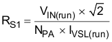
where
- NPA is the transformer primary-to-auxiliary turns-ratio,
- VIN(run) is the AC RMS voltage to enable turnon of the controller (run),
(in case of DC input, leave out the √ 2 term in the equation), - IVSL(run) is the run-threshold for the current pulled out of the VS pin during the switch on-time (see Section 6.5).
Equation 2. 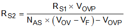
where
- VOV is the maximum allowable peak voltage at the converter output,
- VF is the output-rectifier forward drop at near-zero current,
- NAS is the transformer auxiliary-to-secondary turns-ratio,
- RS1 is the VS divider high-side resistance,
- VOVP is the overvoltage detection threshold at the VS input (see Section 6.5).
- FB (Feedback)The FB pin connects to the emitter of an analog-optocoupler output transistor which usually has the collector connected to VDD. The current supplied to FB by the optocoupler is reduced internally by a factor of 2.5 and the resulting current is applied to an internal 480-kΩ resistor to generate the control law voltage (VCL). This VCL directly determines the converter switching frequency and peak primary current required for regulation per the control-law for any given line and load condition.
- DRV (Gate Drive)The DRV pin connects to the MOSFET gate pin, usually through a series resistor. The gate driver provides a gate-drive signal limited to 14 V. The turnon characteristic of the driver is a 25-mA current source which limits the turnon dv/dt of the MOSFET drain and reduces the leading-edge current spike while still providing a gate-drive current to overcome the Miller plateau. The gate-drive turnoff current is determined by the RDSON of the low-side driver along with any external gate-drive resistance. Adding external gate resistance reduces the MOSFET drain turn-off dv/dt, if necessary.
- CS (Current Sense)The current-sense pin connects through a series resistor (RLC) to the current-sense resistor (RCS). The maximum current-sense threshold (VCST(max)) is 0.773 V for IPP(max), and the minimum current-sense threshold (VCST(min)) is 0.194 V for IPP(min). RLC provides the feed-forward line compensation to eliminate changes in IPP with input voltage due to the propagation delay of the internal comparator and MOSFET turnoff time. An internal leading-edge blanking time of 235 ns eliminates sensitivity to the MOSFET turnon current spike. Placing a bypass capacitor on the CS pin is unnecessary. The target output current in constant-current (CC) regulation determines the value of RCS. The values of RCS and RLC are calculated using Equation 3 and Equation 4. The term VCCR is the product of the demagnetization constant, 0.425, and VCST(max). VCCRis held to a tighter accuracy than either of its constituent terms. The term ηXFMR accounts for the energy stored in the transformer but not delivered to the secondary. This term includes transformer resistance and core loss, bias power, and primary-to-secondary leakage ratio.
Example:
With a transformer core and winding loss of 5%, primary-to-secondary leakage inductance of 3.5%, and bias power to output power ratio of 0.5%, the ηXFMR value at full power is approximately:
1 - 0.05 - 0.035 - 0.005 = 0.91.
Equation 3. 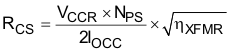
where
- VCCR is a constant-current regulation factor (see Section 6.5),
- NPS is the transformer primary-to-secondary turns-ratio (a ratio of 13 to 15 is typical for 5-V output),
- IOCC is the target output current in constant-current regulation,
- ηXFMR is the transformer efficiency at full power.
Equation 4. 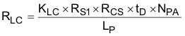
where
- RS1 is the VS pin high-side resistor value,
- RCS is the current-sense resistor value,
- tD is the total current-sense delay consisting of MOSFET turnoff delay, plus approximately 50 ns internal delay,
- NPA is the transformer primary-to-auxiliary turns-ratio,
- LP is the transformer primary inductance,
- KLC is a current-scaling constant for line compensation (see Section 6.5).