SLUSDT2C August 2019 – December 2020 UCC28740-Q1
PRODUCTION DATA
- 1 Features
- 2 Applications
- 3 Description
- 4 Revision History
- 5 Pin Configuration and Functions
- 6 Specifications
- 7 Detailed Description
-
8 Application and Implementation
- 8.1 Application Information
- 8.2 High Voltage Applications
- 8.3
Typical Application
- 8.3.1 Design Requirements
- 8.3.2
Detailed Design Procedure
- 8.3.2.1 Custom Design With WEBENCH® Tools
- 8.3.2.2 Standby Power Estimate and No-Load Switching Frequency
- 8.3.2.3 Input Bulk Capacitance and Minimum Bulk Voltage
- 8.3.2.4 35
- 8.3.2.5 Transformer Turns-Ratio, Inductance, Primary Peak Current
- 8.3.2.6 Transformer Parameter Verification
- 8.3.2.7 VS Resistor Divider, Line Compensation
- 8.3.2.8 Output Capacitance
- 8.3.2.9 VDD Capacitance, CVDD
- 8.3.2.10 Feedback Network Biasing
- 8.3.3 Application Curves
- 9 Power Supply Recommendations
- 10Layout
-
11Device and Documentation Support
- 11.1
Device Support
- 11.1.1 Development Support
- 11.1.2
Device Nomenclature
- 11.1.2.1 Capacitance Terms in Farads
- 11.1.2.2 Duty Cycle Terms
- 11.1.2.3 Frequency Terms in Hertz
- 11.1.2.4 Current Terms in Amperes
- 11.1.2.5 Current and Voltage Scaling Terms
- 11.1.2.6 Transformer Terms
- 11.1.2.7 Power Terms in Watts
- 11.1.2.8 Resistance Terms in Ohms
- 11.1.2.9 Timing Terms in Seconds
- 11.1.2.10 Voltage Terms in Volts
- 11.1.2.11 AC Voltage Terms in VRMS
- 11.1.2.12 Efficiency Terms
- 11.2 Documentation Support
- 11.3 Receiving Notification of Documentation Updates
- 11.4 Community Resources
- 11.5 Trademarks
- 11.1
Device Support
Package Options
Mechanical Data (Package|Pins)
- D|7
Thermal pad, mechanical data (Package|Pins)
Orderable Information
8.3.2.2 Standby Power Estimate and No-Load Switching Frequency
Assuming minimal no-load standby power is a critical design requirement, determine the estimated no-load power loss based on an accounting of all no-load operating and leakage currents at their respective voltages. Close attention to detail is necessary to account for all of the sources of leakage, however, in many cases, prototype measurement is the only means to obtain a realistic estimation of total primary and secondary leakage currents. At present, converter standby power is certified by compliance-agency authorities based on steady-state room-temperature operation at the highest nominal input voltage rating (typically 230 Vrms).
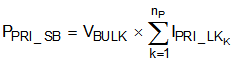
Equation 6 estimates the standby power loss from the sum of all leakage currents of the primary-side components of the converter. These leakage currents are measured in aggregate by disconnecting the HV input of the controller from the bulk-voltage rail to prevent operating currents from interfering with the leakage measurement.
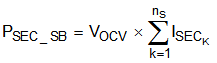
Equation 7 estimates the standby power loss from the sum of all leakage and operating currents of the secondary-side components on the output of the converter. Leakage currents result from reverse voltage applied across the output rectifier and capacitors, while the operating current includes currents required by the shunt-regulator, optocoupler, and associated components.
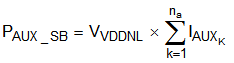
Equation 8 estimates the standby power loss from the sum of all leakage and operating currents of the auxiliary-side components on the controller of the converter. Leakage currents of the auxiliary diode and capacitor are usually negligible. The operating current includes the wait-state current, IWAIT, of the UCC28740-Q1 controller, plus the optocoupler-output current for the FB network in the steady-state no-load condition. The VDD voltage in the no-load condition VVDDNL are the lowest practicable value to minimize loss.
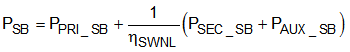
Note that PPRI_SB is the only loss that is not dependent on transformer conversion efficiency. PSEC_SB and PAUX_SB are processed through the transformer and incur additional losses as a consequence. Typically, the transformer no-load conversion efficiency ηSWNL lies in the range of 0.50 to 0.70. Total standby input power (no-load condition) is estimated by Equation 9.
Although the UCC28740-Q1 is capable of operating at the minimum switching frequency of 170 Hz, a typical converter is likely to require a higher frequency to sustain operation at no-load. An accurate estimate of the no-load switching frequency fSWNL entails a thorough accounting of all switching-related energy losses within the converter including parasitic elements of the power-train components. In general, fSWNL is likely to lie within the range of 400 Hz to 800 Hz. A more detailed treatment of standby power and no-load frequency is beyond the scope of this data sheet.