SLUSDT2C August 2019 – December 2020 UCC28740-Q1
PRODUCTION DATA
- 1 Features
- 2 Applications
- 3 Description
- 4 Revision History
- 5 Pin Configuration and Functions
- 6 Specifications
- 7 Detailed Description
-
8 Application and Implementation
- 8.1 Application Information
- 8.2 High Voltage Applications
- 8.3
Typical Application
- 8.3.1 Design Requirements
- 8.3.2
Detailed Design Procedure
- 8.3.2.1 Custom Design With WEBENCH® Tools
- 8.3.2.2 Standby Power Estimate and No-Load Switching Frequency
- 8.3.2.3 Input Bulk Capacitance and Minimum Bulk Voltage
- 8.3.2.4 35
- 8.3.2.5 Transformer Turns-Ratio, Inductance, Primary Peak Current
- 8.3.2.6 Transformer Parameter Verification
- 8.3.2.7 VS Resistor Divider, Line Compensation
- 8.3.2.8 Output Capacitance
- 8.3.2.9 VDD Capacitance, CVDD
- 8.3.2.10 Feedback Network Biasing
- 8.3.3 Application Curves
- 9 Power Supply Recommendations
- 10Layout
-
11Device and Documentation Support
- 11.1
Device Support
- 11.1.1 Development Support
- 11.1.2
Device Nomenclature
- 11.1.2.1 Capacitance Terms in Farads
- 11.1.2.2 Duty Cycle Terms
- 11.1.2.3 Frequency Terms in Hertz
- 11.1.2.4 Current Terms in Amperes
- 11.1.2.5 Current and Voltage Scaling Terms
- 11.1.2.6 Transformer Terms
- 11.1.2.7 Power Terms in Watts
- 11.1.2.8 Resistance Terms in Ohms
- 11.1.2.9 Timing Terms in Seconds
- 11.1.2.10 Voltage Terms in Volts
- 11.1.2.11 AC Voltage Terms in VRMS
- 11.1.2.12 Efficiency Terms
- 11.2 Documentation Support
- 11.3 Receiving Notification of Documentation Updates
- 11.4 Community Resources
- 11.5 Trademarks
- 11.1
Device Support
Package Options
Mechanical Data (Package|Pins)
- D|7
Thermal pad, mechanical data (Package|Pins)
Orderable Information
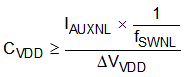
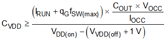
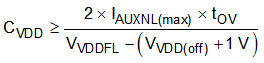
8.3.2.9 VDD Capacitance, CVDD
The capacitance on VDD must supply the primary-side operating current used during startup and between low-frequency switching pulses. The largest result of three independent calculations denoted in Equation 28, Equation 29, and Equation 30 determines the value of CVDD.
At startup, when VVDD(on) is reached, CVDD alone supplies the device operating current and MOSFET gate current until the output of the converter reaches the target minimum-operating voltage in CC regulation, VOCC. Now the auxiliary winding sustains VDD for the UCC28740-Q1 above UVLO. The total output current available to the load and to charge the output capacitors is the CC-regulation target, IOCC. Equation 28 assumes that all of the output current of the converter is available to charge the output capacitance until VOCC is achieved. For typical applications, Equation 28 includes an estimated qGfSW(max) of average gate-drive current and a 1-V margin added to VVDD.
During a worst-case un-load transient event from full-load to no-load, COUT overcharges above the normal regulation level for a duration of tOV, until the output shunt-regulator loading is able to drain VOUT back to regulation. During tOV, the voltage feedback loop and optocoupler are saturated, driving maximum IFB and temporarily switching at fSW(min). The auxiliary bias current expended during this situation exceeds that normally required during the steady-state no-load condition. Equation 29 calculates the value of CVDD (with a safety factor of 2) required to ride through the tOV duration until steady-state no-load operation is achieved.
Finally, in the steady-state no-load operating condition, total no-load auxiliary-bias current, IAUXNL is provided by the converter switching at a no-load frequency, fSWNL, which is generally higher than fSW(min). CVDD is calculated to maintain a target VDD ripple voltage lower than ΔVVDD, using Equation 30.