SLUSBF3D July 2013 – March 2018 UCC28740
PRODUCTION DATA.
- 1 Features
- 2 Applications
- 3 Description
- 4 Revision History
- 5 Pin Configuration and Functions
- 6 Specifications
- 7 Detailed Description
-
8 Application and Implementation
- 8.1 Application Information
- 8.2
Typical Application
- 8.2.1 Design Requirements
- 8.2.2
Detailed Design Procedure
- 8.2.2.1 Custom Design With WEBENCH® Tools
- 8.2.2.2 Standby Power Estimate and No-Load Switching Frequency
- 8.2.2.3 Input Bulk Capacitance and Minimum Bulk Voltage
- 8.2.2.4 Transformer Turns-Ratio, Inductance, Primary Peak Current
- 8.2.2.5 Transformer Parameter Verification
- 8.2.2.6 VS Resistor Divider, Line Compensation
- 8.2.2.7 Output Capacitance
- 8.2.2.8 VDD Capacitance, CVDD
- 8.2.2.9 Feedback Network Biasing
- 8.2.3 Application Curves
- 9 Power Supply Recommendations
- 10Layout
-
11Device and Documentation Support
- 11.1
Device Support
- 11.1.1 Development Support
- 11.1.2
Device Nomenclature
- 11.1.2.1 Capacitance Terms in Farads
- 11.1.2.2 Duty Cycle Terms
- 11.1.2.3 Frequency Terms in Hertz
- 11.1.2.4 Current Terms in Amperes
- 11.1.2.5 Current and Voltage Scaling Terms
- 11.1.2.6 Transformer Terms
- 11.1.2.7 Power Terms in Watts
- 11.1.2.8 Resistance Terms in Ohms
- 11.1.2.9 Timing Terms in Seconds
- 11.1.2.10 Voltage Terms in Volts
- 11.1.2.11 AC Voltage Terms in VRMS
- 11.1.2.12 Efficiency Terms
- 11.2 Documentation Support
- 11.3 Receiving Notification of Documentation Updates
- 11.4 Community Resources
- 11.5 Trademarks
- 11.6 Electrostatic Discharge Caution
- 11.7 Glossary
- 11.1
Device Support
- 12Mechanical, Packaging, and Orderable Information
Package Options
Mechanical Data (Package|Pins)
- D|7
Thermal pad, mechanical data (Package|Pins)
Orderable Information
7.4.1 Secondary-Side Optically Coupled Constant-Voltage (CV) Regulation
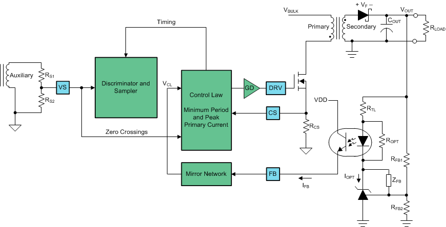
Figure 12 shows a simplified flyback convertor with the main output-regulation blocks of the device shown, along with typical implementation of secondary-side-derived regulation. The power-train operation is the same as any DCM-flyback circuit. A feedback current is optically coupled to the controller from a shunt-regulator sensing the output voltage.
 Figure 12. Simplified Flyback Convertor
(With the Main Voltage Regulation Blocks)
In this configuration, a secondary-side shunt-regulator, such as the TL431, generates a current through the input photo-diode of an optocoupler. The photo-transistor delivers a proportional current that is dependent on the current-transfer ratio (CTR) of the optocoupler to the FB input of the UCC28740 controller. This FB current then converts into the VCL by the input-mirror network, detailed in the device block diagram (see Functional Block Diagram). Output-voltage variations convert to FB-current variations. The FB-current variations modify the VCL which dictates the appropriate IPP and fSW necessary to maintain CV regulation. At the same time, the VS input senses the auxiliary winding voltage during the transfer of transformer energy to the secondary output to monitor for an output overvoltage condition. When fSW reaches the target maximum frequency, chosen between 32 kHz and 100 kHz, CC operation is entered and further increases in VCL have no effect.
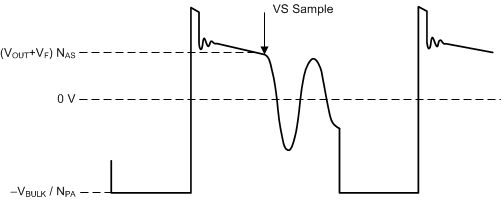
Figure 13 shows that as the secondary current decreases to zero, a clearly defined down slope reflects the decreasing rectifier VF combined with stray resistance voltage-drop (ISRS). To achieve an accurate representation of the secondary output voltage on the auxiliary winding, the discriminator reliably blocks the leakage-inductance reset and ringing while continuously sampling the auxiliary voltage during the down slope after the ringing diminishes. The discriminator then captures the voltage signal at the moment that the secondary-winding current reaches zero. The internal overvoltage threshold on VS is 4.6 V. Temperature compensation of –0.8 mV/°C on the overvoltage threshold offsets the change in the output-rectifier forward voltage with temperature. The resistor divider is selected as outlined in the VS pin description (see Detailed Pin Description).
 Figure 13. Auxiliary-Winding Voltage
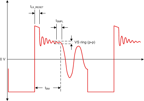
The UCC28740 VS-signal sampler includes signal-discrimination methods to ensure an accurate sample of the output voltage from the auxiliary winding. Controlling some details of the auxiliary-winding signal to ensure reliable operation is necessary; specifically, the reset time of the leakage inductance and the duration of any subsequent leakage-inductance ringing. See Figure 14 for a detailed illustration of waveform criteria to ensure a reliable sample on the VS pin.
The first detail to examine is the duration of the leakage-inductance reset pedestal, tLK_RESET, in Figure 14. Because tLK_RESET mimics the waveform of the secondary-current decay, followed by a sharp downslope, tLK_RESET is internally blanked for a duration which scales with the peak primary current. Keeping the leakage-reset time to less than 600 ns for IPP(min), and less than 2.2 µs for IPP(max) is important.
The second detail is the amplitude of ringing on the VAUX waveform following tLK_RESET. The peak-to-peak voltage variation at the VS pin must be less than 100 mVp-p for at least 200 ns before the end of the demagnetization time (tDM). A concern with excessive ringing usually occurs during light or no-load conditions, when tDM is at the minimum. The tolerable ripple on VS is scaled up to the auxiliary-winding voltage by RS1 and RS2, and is equal to 100 mV × (RS1 + RS2) / RS2.
 Figure 14. Auxiliary-Winding Waveform Details
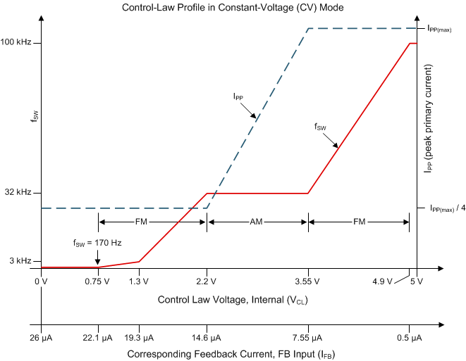
During voltage regulation, the controller operates in frequency-modulation mode and amplitude-modulation mode, as shown in Figure 15. The internal operating-frequency limits of the device are 100 kHz and fSW(min). The maximum operating frequency of the converter at full-load is generally chosen to be slightly lower than 100 kHz to allow for tolerances, or significantly lower due to switching-loss considerations. The maximum operating frequency and primary peak current chosen determine the transformer primary inductance of the converter. The shunt-regulator bias power, output preload resistor (if any), and low-power conversion efficiency determine the minimum-operating frequency of the converter. Voltage-loop stability compensation is applied at the shunt-regulator which drives the opto-coupled feedback signal. The tolerances chosen for the shunt-regulator reference and the sense resistors determines the regulation accuracy.
 Figure 15. Frequency and Amplitude Modulation Modes
(During CV Regulation)
The level of feedback current (IFB) into the FB pin determines the internal VCL which determines the operating point of the controller while in CV mode. When IFB rises above 22 µA, no further decrease in fSW occurs. When the output-load current increases to the point where maximum fSW is reached, control transfers to CC mode. All current, voltage, frequency, breakpoints, and curve-segment linearity depicted in Figure 15 are nominal. Figure 15 indicates the general operation of the controller while in CV mode, although minor variations may occur from part to part. An internal frequency-dithering mechanism is enabled when IFB is less than 14.6 µA to help reduce conducted EMI (including during CC-mode operation), and is disabled otherwise.