SLUSDK4E may 2020 – july 2023 UCC28782
PRODUCTION DATA
- 1
- 1 Features
- 2 Applications
- 3 Description
- 4 Revision History
- 5 Device Comparison Table
- 6 Pin Configuration and Functions
- 7 Specifications
-
8 Detailed Description
- 8.1 Overview
- 8.2 Functional Block Diagram
- 8.3
Detailed Pin Description
- 8.3.1 BUR Pin (Programmable Burst Mode)
- 8.3.2 FB Pin (Feedback Pin)
- 8.3.3 REF Pin (Internal 5-V Bias)
- 8.3.4 VDD Pin (Device Bias Supply)
- 8.3.5 P13 and SWS Pins
- 8.3.6 S13 Pin
- 8.3.7 IPC Pin (Intelligent Power Control Pin)
- 8.3.8 RUN Pin (Driver and Bias Source for Isolator)
- 8.3.9 PWMH and AGND Pins
- 8.3.10 PWML and PGND Pins
- 8.3.11 SET Pin
- 8.3.12 RTZ Pin (Sets Delay for Transition Time to Zero)
- 8.3.13 RDM Pin (Sets Synthesized Demagnetization Time for ZVS Tuning)
- 8.3.14 BIN, BSW, and BGND Pins
- 8.3.15 XCD Pin
- 8.3.16 CS, VS, and FLT Pins
- 8.4
Device Functional Modes
- 8.4.1 Adaptive ZVS Control with Auto-Tuning
- 8.4.2 Dead-Time Optimization
- 8.4.3 EMI Dither and Dither Fading Function
- 8.4.4 Control Law across Entire Load Range
- 8.4.5 Adaptive Amplitude Modulation (AAM)
- 8.4.6 Adaptive Burst Mode (ABM)
- 8.4.7 Low Power Mode (LPM)
- 8.4.8 First Standby Power Mode (SBP1)
- 8.4.9 Second Standby Power Mode (SBP2)
- 8.4.10 Startup Sequence
- 8.4.11 Survival Mode of VDD (INT_STOP)
- 8.4.12 Capacitor Voltage Balancing Function
- 8.4.13 Device Functional Modes for Bias Regulator Control
- 8.4.14
System Fault Protections
- 8.4.14.1 Brown-In and Brown-Out
- 8.4.14.2 Output Over-Voltage Protection (OVP)
- 8.4.14.3 Input Over Voltage Protection (IOVP)
- 8.4.14.4 Over-Temperature Protection (OTP) on FLT Pin
- 8.4.14.5 Over-Temperature Protection (OTP) on CS Pin
- 8.4.14.6 Programmable Over-Power Protection (OPP)
- 8.4.14.7 Peak Power Limit (PPL)
- 8.4.14.8 Output Short-Circuit Protection (SCP)
- 8.4.14.9 Over-Current Protection (OCP)
- 8.4.14.10 External Shutdown
- 8.4.14.11 Internal Thermal Shutdown
- 8.4.15 Pin Open/Short Protections
-
9 Application and Implementation
- 9.1 Application Information
- 9.2
Typical Application Circuit
- 9.2.1 Design Requirements for a 65-W USB-PD Adapter Application
- 9.2.2
Detailed Design Procedure
- 9.2.2.1 Input Bulk Capacitance and Minimum Bulk Voltage
- 9.2.2.2 Transformer Calculations
- 9.2.2.3 Clamp Capacitor Calculation
- 9.2.2.4 Bleed-Resistor Calculation
- 9.2.2.5 Output Filter Calculation
- 9.2.2.6 Calculation of ZVS Sensing Network
- 9.2.2.7 Calculation of BUR Pin Resistances
- 9.2.2.8 Calculation of Compensation Network
- 9.2.3 Application Curves
- 10Power Supply Recommendations
- 11Layout
- 12Device and Documentation Support
- 13Mechanical, Packaging, and Orderable Information
Package Options
Mechanical Data (Package|Pins)
- RTW|24
Thermal pad, mechanical data (Package|Pins)
- RTW|24
Orderable Information
9.2.2.5 Output Filter Calculation
The bulk output capacitor of active clamp flyback (ACF) converters, CO1 of the primary-resonance ACF or CO2 of the secondary-resonance ACF, is often determined by the load-step transient-response requirement from no-load to full-load transition. For a target output voltage undershoot (ΔVO) with the load step-up transient of ΔIO, the minimum bulk output capacitance (CO(MIN)) can be expressed as
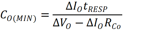
where tRESP is the response time delay from the moment ΔIO is applied to the moment when IFB falls below 10 μA. At ~10 μA, full power is available to prevent further drop of VO and to recharge CO. The response delay time consists of the time for the secondary regulator to stop driving the opto-coupler input plus the time for the opto-coupler output transistor to turn off. RCo is the equivalent series resistance (ESR) of the output capacitor CO.
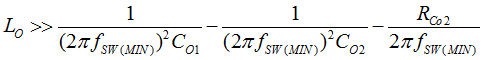
The output filter inductor (LO) is an essential component for the secondary-resonance ACF, not only to filter the large switching voltage ripple across CO1 but also to decouple the effect of CO2 on the resonant period. The sum of LO impedance, ESR of CO2 (RCo2), and CO2 impedance at minimum switching frequency (fSW(MIN)) must be much higher than CO1 impedance at the same frequency to force most of switching resonant current to flow through CO1 only. LO is chosen with minimal ESR to achieve minimal conduction loss.
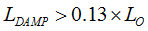
One benefit of lowering the ESR on CO1 (RCo1) is to help to reduce the switching ripple on the output voltage. Another benefit is reducing the conduction loss of CO1 for the secondary-resonance ACF converter. However, the issue is that the damping between LO and CO1 is weakened. Without proper damping, the magnitude of low-frequency resonant ripple between LO and CO1 enlarges output ripple, affects the loop stability, and affects the operation of synchronous rectifier (QSEC). The secondary-resonance ACF converter is the most vulnerable since CO1 with low capacitance significantly weakens the damping. To resolve this issue, it is found that a serial damping network formed by LDAMP and RDAMP is a very effective way to minimize the impact. However, too much damping results in noticeable conduction loss increase and full-load efficiency drop. Therefore, it is recommended that LDAMP and RDAMP should be higher than the theoretical strong damping value as the following equations suggest. Even though the damping network is an additional component, the physical size or the footprint is much smaller than LO, not only because of the small value but also the wide availability of small-size chip inductors with high winding resistance can provide "free" RDAMP. For the 65-W secondary-resonance ACF design with primary GaN FETs and a polymer-type CO2, when a 0.68-µH chip inductor is in parallel with a 1-µH output filter inductor, there is only 0.15% full-load efficiency drop at 90-V AC input, and there is a negligible efficiency difference at 230-V AC input.
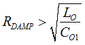
The equation for RDAMP assumes that CO2 >> CO1. Select a standard component available with parameter values that satisfy both of these two equations. It is usually not necessary to use two separate components.