SLUSDK4E may 2020 – july 2023 UCC28782
PRODUCTION DATA
- 1
- 1 Features
- 2 Applications
- 3 Description
- 4 Revision History
- 5 Device Comparison Table
- 6 Pin Configuration and Functions
- 7 Specifications
-
8 Detailed Description
- 8.1 Overview
- 8.2 Functional Block Diagram
- 8.3
Detailed Pin Description
- 8.3.1 BUR Pin (Programmable Burst Mode)
- 8.3.2 FB Pin (Feedback Pin)
- 8.3.3 REF Pin (Internal 5-V Bias)
- 8.3.4 VDD Pin (Device Bias Supply)
- 8.3.5 P13 and SWS Pins
- 8.3.6 S13 Pin
- 8.3.7 IPC Pin (Intelligent Power Control Pin)
- 8.3.8 RUN Pin (Driver and Bias Source for Isolator)
- 8.3.9 PWMH and AGND Pins
- 8.3.10 PWML and PGND Pins
- 8.3.11 SET Pin
- 8.3.12 RTZ Pin (Sets Delay for Transition Time to Zero)
- 8.3.13 RDM Pin (Sets Synthesized Demagnetization Time for ZVS Tuning)
- 8.3.14 BIN, BSW, and BGND Pins
- 8.3.15 XCD Pin
- 8.3.16 CS, VS, and FLT Pins
- 8.4
Device Functional Modes
- 8.4.1 Adaptive ZVS Control with Auto-Tuning
- 8.4.2 Dead-Time Optimization
- 8.4.3 EMI Dither and Dither Fading Function
- 8.4.4 Control Law across Entire Load Range
- 8.4.5 Adaptive Amplitude Modulation (AAM)
- 8.4.6 Adaptive Burst Mode (ABM)
- 8.4.7 Low Power Mode (LPM)
- 8.4.8 First Standby Power Mode (SBP1)
- 8.4.9 Second Standby Power Mode (SBP2)
- 8.4.10 Startup Sequence
- 8.4.11 Survival Mode of VDD (INT_STOP)
- 8.4.12 Capacitor Voltage Balancing Function
- 8.4.13 Device Functional Modes for Bias Regulator Control
- 8.4.14
System Fault Protections
- 8.4.14.1 Brown-In and Brown-Out
- 8.4.14.2 Output Over-Voltage Protection (OVP)
- 8.4.14.3 Input Over Voltage Protection (IOVP)
- 8.4.14.4 Over-Temperature Protection (OTP) on FLT Pin
- 8.4.14.5 Over-Temperature Protection (OTP) on CS Pin
- 8.4.14.6 Programmable Over-Power Protection (OPP)
- 8.4.14.7 Peak Power Limit (PPL)
- 8.4.14.8 Output Short-Circuit Protection (SCP)
- 8.4.14.9 Over-Current Protection (OCP)
- 8.4.14.10 External Shutdown
- 8.4.14.11 Internal Thermal Shutdown
- 8.4.15 Pin Open/Short Protections
-
9 Application and Implementation
- 9.1 Application Information
- 9.2
Typical Application Circuit
- 9.2.1 Design Requirements for a 65-W USB-PD Adapter Application
- 9.2.2
Detailed Design Procedure
- 9.2.2.1 Input Bulk Capacitance and Minimum Bulk Voltage
- 9.2.2.2 Transformer Calculations
- 9.2.2.3 Clamp Capacitor Calculation
- 9.2.2.4 Bleed-Resistor Calculation
- 9.2.2.5 Output Filter Calculation
- 9.2.2.6 Calculation of ZVS Sensing Network
- 9.2.2.7 Calculation of BUR Pin Resistances
- 9.2.2.8 Calculation of Compensation Network
- 9.2.3 Application Curves
- 10Power Supply Recommendations
- 11Layout
- 12Device and Documentation Support
- 13Mechanical, Packaging, and Orderable Information
Package Options
Mechanical Data (Package|Pins)
- RTW|24
Thermal pad, mechanical data (Package|Pins)
- RTW|24
Orderable Information
8.4.4 Control Law across Entire Load Range
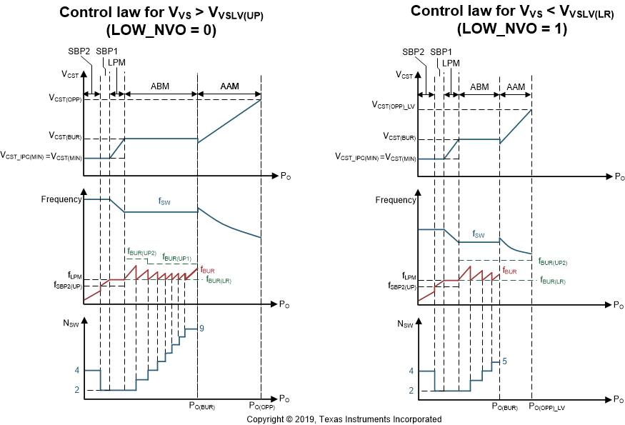
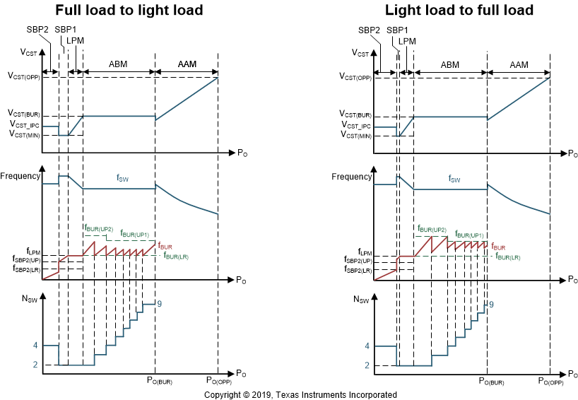
UCC28782 contains six modes of operation summarized in Table 8-1. Starting from heavier load, the AAM mode forces PWML and PWMH into complementary switching with ZVS tuning enabled. ABM mode generates a group of PWML and PWMH pulses as a burst packet, and adjusts the burst off-time to regulate the output voltage. At the same time, the burst frequency variation is confined above 20kHz by adjusting the number of PWML and PWMH pulses per packet to mitigate audible noise and reduce burst output ripple. In LPM, SBP1, and SBP2 modes, PWMH and the ZVS tuning loop are disabled, so the converter operates in valley-switching. The survival mode is to maintain VVDD higher than VVDD(OFF) in a long burst off time, and also performs the clamping capacitor balancing function to reduce the voltage stress of the secondary-side rectifier.
| MODE | OPERATION | PWMH | ZVS | |
|---|---|---|---|---|
| AAM | Adaptive Amplitude Modulation | ACF operation with PWML and PWMH in complementary switching | Enabled | Yes |
| ABM | Adaptive Burst Mode | Variable fBUR > fBUR(LR), ACF operation in complementary switching | Enabled | Yes |
| LPM | Low Power Mode | Fix fBUR ≈ fLPM, valley-switching | Disabled | No |
| SBP1 | First StandBy Power Mode | Variable fBUR between fSBP2(LR) and fSBP2(UP), valley-switching | Disabled | No |
| SBP2 | Second StandBy Power Mode | Variable fBUR < fSBP2(UP) as VBUR < 0.9 V; Variable fBUR < fSBP2(LR) as VBUR > 0.9 V; Both are in valley-switching | Disabled | No |
| INT_STOP | Survival Mode | When VVDD < VVDD(OFF) + VVDD(PCT), a series of PWML pulses followed by a long PWMH pulse is generated | Enabled in the last switching cycle of a survival-mode burst packet | No |
Figure 8-24 and Figure 8-25 show the critical parameter changes among the five operating modes, where VCST is the peak current threshold compared with the current-sense voltage from the CS pin, fSW is the switching frequency of PWML, fBUR is the burst frequency, and NSW is the pulse number of PWML cycles per burst packet. Figure 8-24 represents the control mode difference under the two VS-pin voltage ranges, when the IPC-pin voltage is less than 0.9 V or IPC is connected to AGND. Figure 8-25 illustrates the modified control mode, when the IPC-pin voltage setting is higher than 0.9 V. The following section explains the detailed operation of each mode. The VS-pin voltage and IPC-pin voltage effects will also be introduced in the following section.
 Figure 8-24 Control Law Over Entire Load Range Based on the VVS Condition as VIPC < 0.9 V
 Figure 8-25 Control Law Under Different Load Sweep Direction as VIPC > 0.9 V and VVS > VVSLV(UP)