SLUSDK4E may 2020 – july 2023 UCC28782
PRODUCTION DATA
- 1
- 1 Features
- 2 Applications
- 3 Description
- 4 Revision History
- 5 Device Comparison Table
- 6 Pin Configuration and Functions
- 7 Specifications
-
8 Detailed Description
- 8.1 Overview
- 8.2 Functional Block Diagram
- 8.3
Detailed Pin Description
- 8.3.1 BUR Pin (Programmable Burst Mode)
- 8.3.2 FB Pin (Feedback Pin)
- 8.3.3 REF Pin (Internal 5-V Bias)
- 8.3.4 VDD Pin (Device Bias Supply)
- 8.3.5 P13 and SWS Pins
- 8.3.6 S13 Pin
- 8.3.7 IPC Pin (Intelligent Power Control Pin)
- 8.3.8 RUN Pin (Driver and Bias Source for Isolator)
- 8.3.9 PWMH and AGND Pins
- 8.3.10 PWML and PGND Pins
- 8.3.11 SET Pin
- 8.3.12 RTZ Pin (Sets Delay for Transition Time to Zero)
- 8.3.13 RDM Pin (Sets Synthesized Demagnetization Time for ZVS Tuning)
- 8.3.14 BIN, BSW, and BGND Pins
- 8.3.15 XCD Pin
- 8.3.16 CS, VS, and FLT Pins
- 8.4
Device Functional Modes
- 8.4.1 Adaptive ZVS Control with Auto-Tuning
- 8.4.2 Dead-Time Optimization
- 8.4.3 EMI Dither and Dither Fading Function
- 8.4.4 Control Law across Entire Load Range
- 8.4.5 Adaptive Amplitude Modulation (AAM)
- 8.4.6 Adaptive Burst Mode (ABM)
- 8.4.7 Low Power Mode (LPM)
- 8.4.8 First Standby Power Mode (SBP1)
- 8.4.9 Second Standby Power Mode (SBP2)
- 8.4.10 Startup Sequence
- 8.4.11 Survival Mode of VDD (INT_STOP)
- 8.4.12 Capacitor Voltage Balancing Function
- 8.4.13 Device Functional Modes for Bias Regulator Control
- 8.4.14
System Fault Protections
- 8.4.14.1 Brown-In and Brown-Out
- 8.4.14.2 Output Over-Voltage Protection (OVP)
- 8.4.14.3 Input Over Voltage Protection (IOVP)
- 8.4.14.4 Over-Temperature Protection (OTP) on FLT Pin
- 8.4.14.5 Over-Temperature Protection (OTP) on CS Pin
- 8.4.14.6 Programmable Over-Power Protection (OPP)
- 8.4.14.7 Peak Power Limit (PPL)
- 8.4.14.8 Output Short-Circuit Protection (SCP)
- 8.4.14.9 Over-Current Protection (OCP)
- 8.4.14.10 External Shutdown
- 8.4.14.11 Internal Thermal Shutdown
- 8.4.15 Pin Open/Short Protections
-
9 Application and Implementation
- 9.1 Application Information
- 9.2
Typical Application Circuit
- 9.2.1 Design Requirements for a 65-W USB-PD Adapter Application
- 9.2.2
Detailed Design Procedure
- 9.2.2.1 Input Bulk Capacitance and Minimum Bulk Voltage
- 9.2.2.2 Transformer Calculations
- 9.2.2.3 Clamp Capacitor Calculation
- 9.2.2.4 Bleed-Resistor Calculation
- 9.2.2.5 Output Filter Calculation
- 9.2.2.6 Calculation of ZVS Sensing Network
- 9.2.2.7 Calculation of BUR Pin Resistances
- 9.2.2.8 Calculation of Compensation Network
- 9.2.3 Application Curves
- 10Power Supply Recommendations
- 11Layout
- 12Device and Documentation Support
- 13Mechanical, Packaging, and Orderable Information
Package Options
Mechanical Data (Package|Pins)
- RTW|24
Thermal pad, mechanical data (Package|Pins)
- RTW|24
Orderable Information
9.2.2.2.5 Auxiliary Winding Turns (NA)
Turns of the auxiliary winding (NA) is an integer value usually chosen to provide a nominal VVDD that satisfies all devices powered from VVDD, such as a gate driver, UCC28782, etc. NA is determined by the following design considerations:
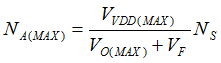
- VVDD must be lower than the maximum rating voltage of VDD pin (VVDD(MAX)) at maximum output voltage and rectifier forward drop (VO(MAX) + VF). VVDD(MAX) is also limited by the lowest voltage rating of any other devices connected to the VDD pin. Use the lower result of the two following options, where applicable.
- For designs with a fixed output voltage or a narrow output range, the maximum Auxiliary winding turns (NA(MAX)) is given by the following equation.
Equation 36.
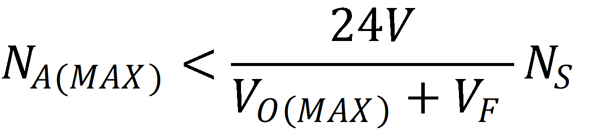
- For designs with wide-output voltage range (such as with USB-PD or PPS or similar) where the boost circuit is likely to be used, leakage inductance may peak-charge the BIN capacitance. The internal boost switch has a maximum rating of 30 V, so a 24-V Zener diode is often used as a clamping device to avoid overstress on BSW. This clamping voltage sets a lower limit on NA(MAX) and is given by the following equation.
Equation 37.
- For designs with a fixed output voltage or a narrow output range, the maximum Auxiliary winding turns (NA(MAX)) is given by the following equation.
- The nominal VVDD should consider the impact on the stand-by power. Higher VVDD results in a static-loss increase with the total bias current of the devices connected to the VDD pin.
- VVDD should be higher than the 13-V threshold voltage of survival mode (which is the sum of VVDD(OFF) and VVDD(PCT)) at the minimum sustained output voltage (VO(MIN)). ΔV here represents the voltage difference between the nominal VVDD and the survival-mode threshold. A minimum of 3 V is a recommended design margin for ΔV.
Equation 38.
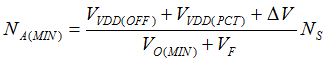
NA(MIN) must also accommodate the highest VVDD(OFF) threshold of other devices powered by VDD, if any. Select an integer value for NA between the lowest NA(MAX) and the highest NA(MIN) with consideration of #2. For best performance, design the DC resistance of the auxiliary winding to be < 0.1 Ω.