SLUSDK4E may 2020 – july 2023 UCC28782
PRODUCTION DATA
- 1
- 1 Features
- 2 Applications
- 3 Description
- 4 Revision History
- 5 Device Comparison Table
- 6 Pin Configuration and Functions
- 7 Specifications
-
8 Detailed Description
- 8.1 Overview
- 8.2 Functional Block Diagram
- 8.3
Detailed Pin Description
- 8.3.1 BUR Pin (Programmable Burst Mode)
- 8.3.2 FB Pin (Feedback Pin)
- 8.3.3 REF Pin (Internal 5-V Bias)
- 8.3.4 VDD Pin (Device Bias Supply)
- 8.3.5 P13 and SWS Pins
- 8.3.6 S13 Pin
- 8.3.7 IPC Pin (Intelligent Power Control Pin)
- 8.3.8 RUN Pin (Driver and Bias Source for Isolator)
- 8.3.9 PWMH and AGND Pins
- 8.3.10 PWML and PGND Pins
- 8.3.11 SET Pin
- 8.3.12 RTZ Pin (Sets Delay for Transition Time to Zero)
- 8.3.13 RDM Pin (Sets Synthesized Demagnetization Time for ZVS Tuning)
- 8.3.14 BIN, BSW, and BGND Pins
- 8.3.15 XCD Pin
- 8.3.16 CS, VS, and FLT Pins
- 8.4
Device Functional Modes
- 8.4.1 Adaptive ZVS Control with Auto-Tuning
- 8.4.2 Dead-Time Optimization
- 8.4.3 EMI Dither and Dither Fading Function
- 8.4.4 Control Law across Entire Load Range
- 8.4.5 Adaptive Amplitude Modulation (AAM)
- 8.4.6 Adaptive Burst Mode (ABM)
- 8.4.7 Low Power Mode (LPM)
- 8.4.8 First Standby Power Mode (SBP1)
- 8.4.9 Second Standby Power Mode (SBP2)
- 8.4.10 Startup Sequence
- 8.4.11 Survival Mode of VDD (INT_STOP)
- 8.4.12 Capacitor Voltage Balancing Function
- 8.4.13 Device Functional Modes for Bias Regulator Control
- 8.4.14
System Fault Protections
- 8.4.14.1 Brown-In and Brown-Out
- 8.4.14.2 Output Over-Voltage Protection (OVP)
- 8.4.14.3 Input Over Voltage Protection (IOVP)
- 8.4.14.4 Over-Temperature Protection (OTP) on FLT Pin
- 8.4.14.5 Over-Temperature Protection (OTP) on CS Pin
- 8.4.14.6 Programmable Over-Power Protection (OPP)
- 8.4.14.7 Peak Power Limit (PPL)
- 8.4.14.8 Output Short-Circuit Protection (SCP)
- 8.4.14.9 Over-Current Protection (OCP)
- 8.4.14.10 External Shutdown
- 8.4.14.11 Internal Thermal Shutdown
- 8.4.15 Pin Open/Short Protections
-
9 Application and Implementation
- 9.1 Application Information
- 9.2
Typical Application Circuit
- 9.2.1 Design Requirements for a 65-W USB-PD Adapter Application
- 9.2.2
Detailed Design Procedure
- 9.2.2.1 Input Bulk Capacitance and Minimum Bulk Voltage
- 9.2.2.2 Transformer Calculations
- 9.2.2.3 Clamp Capacitor Calculation
- 9.2.2.4 Bleed-Resistor Calculation
- 9.2.2.5 Output Filter Calculation
- 9.2.2.6 Calculation of ZVS Sensing Network
- 9.2.2.7 Calculation of BUR Pin Resistances
- 9.2.2.8 Calculation of Compensation Network
- 9.2.3 Application Curves
- 10Power Supply Recommendations
- 11Layout
- 12Device and Documentation Support
- 13Mechanical, Packaging, and Orderable Information
Package Options
Mechanical Data (Package|Pins)
- RTW|24
Thermal pad, mechanical data (Package|Pins)
- RTW|24
Orderable Information
8.3.12 RTZ Pin (Sets Delay for Transition Time to Zero)
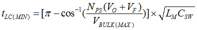
The dead-time between PWMH falling edge and PWML rising edge (tZ) serves as the wait time for VSW transition from its high level down to the target ZVS point. Since the optimal tZ varies with VBULK, the internal dead-time optimizer automatically extends tZ as VBULK is less than the highest voltage of the input bulk capacitor (VBULK(MAX)). The circulating energy for ZVS can be further reduced, obtaining higher efficiency at low line versus a fixed dead-time over a wide line voltage range. A resistor on the RTZ pin (RRTZ) programs the minimum tZ (tZ(MIN)) at VBULK(MAX), which is the sum of the propagation delay of the high-side driver (tD(DR)) and the minimum resonant transition time of VSW falling edge (tLC(MIN)).
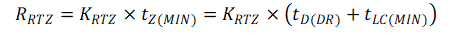
where KRTZ is equal to 11.2×10¹¹ (unit: F-1) for VSET = 0 V, and 5.6×10¹¹(unit: F-1) for VSET = 5 V.
 Figure 8-14 RTZ Setting for the Falling-edge Transition of VSW
As illustrated in Figure 8-14, when PWMH turns off QH after tD(DR) delay, the negative magnetizing current (iM-) becomes an initial condition of the resonant tank formed by magnetizing inductance (LM) and the switch-node capacitance (CSW). CSW is the total capacitive loading on the switch-node, including all junction capacitance (COSS) of switching devices, stray capacitance of the boot-strap diode, intra-winding capacitance of the transformer, the snubber capacitor, and parasitic capacitance of the PCB traces between switch-node and ground. Unlike a conventional valley-switching flyback converter, the resonance of an active clamp flyback converter at high line does not begin at the peak of the sinusoidal trajectory. The transition time of VSW takes less than half of the resonant period. The following tLC(MIN) expression quantifies the transition time for RRTZ calculation, where an arccosine term represents the initial angle at the beginning of resonance. As an example, the value of π minus the arccosine term at VBULK(MAX) of 375 V, VO of 20 V, and NPS of 5 is around 0.585π, which is close to one quarter of the resonant period.