SLUSDK4E may 2020 – july 2023 UCC28782
PRODUCTION DATA
- 1
- 1 Features
- 2 Applications
- 3 Description
- 4 Revision History
- 5 Device Comparison Table
- 6 Pin Configuration and Functions
- 7 Specifications
-
8 Detailed Description
- 8.1 Overview
- 8.2 Functional Block Diagram
- 8.3
Detailed Pin Description
- 8.3.1 BUR Pin (Programmable Burst Mode)
- 8.3.2 FB Pin (Feedback Pin)
- 8.3.3 REF Pin (Internal 5-V Bias)
- 8.3.4 VDD Pin (Device Bias Supply)
- 8.3.5 P13 and SWS Pins
- 8.3.6 S13 Pin
- 8.3.7 IPC Pin (Intelligent Power Control Pin)
- 8.3.8 RUN Pin (Driver and Bias Source for Isolator)
- 8.3.9 PWMH and AGND Pins
- 8.3.10 PWML and PGND Pins
- 8.3.11 SET Pin
- 8.3.12 RTZ Pin (Sets Delay for Transition Time to Zero)
- 8.3.13 RDM Pin (Sets Synthesized Demagnetization Time for ZVS Tuning)
- 8.3.14 BIN, BSW, and BGND Pins
- 8.3.15 XCD Pin
- 8.3.16 CS, VS, and FLT Pins
- 8.4
Device Functional Modes
- 8.4.1 Adaptive ZVS Control with Auto-Tuning
- 8.4.2 Dead-Time Optimization
- 8.4.3 EMI Dither and Dither Fading Function
- 8.4.4 Control Law across Entire Load Range
- 8.4.5 Adaptive Amplitude Modulation (AAM)
- 8.4.6 Adaptive Burst Mode (ABM)
- 8.4.7 Low Power Mode (LPM)
- 8.4.8 First Standby Power Mode (SBP1)
- 8.4.9 Second Standby Power Mode (SBP2)
- 8.4.10 Startup Sequence
- 8.4.11 Survival Mode of VDD (INT_STOP)
- 8.4.12 Capacitor Voltage Balancing Function
- 8.4.13 Device Functional Modes for Bias Regulator Control
- 8.4.14
System Fault Protections
- 8.4.14.1 Brown-In and Brown-Out
- 8.4.14.2 Output Over-Voltage Protection (OVP)
- 8.4.14.3 Input Over Voltage Protection (IOVP)
- 8.4.14.4 Over-Temperature Protection (OTP) on FLT Pin
- 8.4.14.5 Over-Temperature Protection (OTP) on CS Pin
- 8.4.14.6 Programmable Over-Power Protection (OPP)
- 8.4.14.7 Peak Power Limit (PPL)
- 8.4.14.8 Output Short-Circuit Protection (SCP)
- 8.4.14.9 Over-Current Protection (OCP)
- 8.4.14.10 External Shutdown
- 8.4.14.11 Internal Thermal Shutdown
- 8.4.15 Pin Open/Short Protections
-
9 Application and Implementation
- 9.1 Application Information
- 9.2
Typical Application Circuit
- 9.2.1 Design Requirements for a 65-W USB-PD Adapter Application
- 9.2.2
Detailed Design Procedure
- 9.2.2.1 Input Bulk Capacitance and Minimum Bulk Voltage
- 9.2.2.2 Transformer Calculations
- 9.2.2.3 Clamp Capacitor Calculation
- 9.2.2.4 Bleed-Resistor Calculation
- 9.2.2.5 Output Filter Calculation
- 9.2.2.6 Calculation of ZVS Sensing Network
- 9.2.2.7 Calculation of BUR Pin Resistances
- 9.2.2.8 Calculation of Compensation Network
- 9.2.3 Application Curves
- 10Power Supply Recommendations
- 11Layout
- 12Device and Documentation Support
- 13Mechanical, Packaging, and Orderable Information
Package Options
Mechanical Data (Package|Pins)
- RTW|24
Thermal pad, mechanical data (Package|Pins)
- RTW|24
Orderable Information
9.2.2.8 Calculation of Compensation Network
UCC28782 integrates two control concepts to benefit high-efficiency operation: peak current-mode control and burst-ripple control. The peak current loop in AAM can be analyzed based on the linear control theory, so the compensation target is to obtain enough phase margin and gain margin for the given small-signal characteristic of an active clamp flyback converter. For Transition-Mode operation, the power stage can be modeled as a voltage-controlled current source charging an output capacitor (CO) with an equivalent-series resistance (RCo) and the output load (RO) as shown in Figure 9-2. The first-order plant characteristic and high switching frequency operation in AAM make the peak current loop easier to stabilize than ABM.
 Figure 9-2 Small-Signal Model of ACF in AAM Loop
The adaptive burst mode (ABM) uses ripple-based control, so the linear control theory for AAM cannot be applied. As illustrated in Figure 8-4, the internal ramp compensation feature of UCC28782 stabilizes the ABM control loop, so the external compensation network can be simplified.
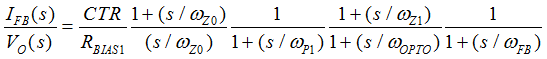
") Figure 9-3 Compensation Network, Hv(s)
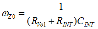
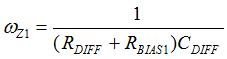
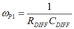
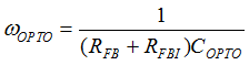
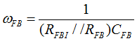
Figure 9-3 Compensation Network, Hv(s)The transfer function from IFB to VO guides the pole/zero placement of the general secondary-side compensation network in Figure 9-3. In the primary-side control circuitry, two poles at ωFB and ωOPTO introduce phase-delay on IFB. ωFB pole is formed by the external filter capacitor CFB and the parallel resistance of the internal RFBI and the external current-limiting resistor (RFB). ωOPTO pole is formed by the parasitic capacitance of the optocoupler output (COPTO) and the series resistance of RFBI and RFB. For CFB = 220 pF, RFBI = 8 KΩ, and RFB = 20 KΩ, the delay effect of ωFB pole located at 139 kHz is negligible. COPTO is in the range of a few nF contributed by the Miller effect of the collector-to-base capacitance of the BJT in the optocoupler output, so ωOPTO pole is located at less than 10 kHz. If the control loop bandwidth needs to be designed at higher frequency for a faster transient response, the phase delay effect of ωOPTO on the stability margin must be taken into account. Therefore, an RC network (RDIFF and CDIFF) in parallel with RBIAS1 is used to compensate the phase-delay of the optocoupler, which introduces an extra pole/zero pair located at ωP1 and ωZ1 respectively. The basic design guide is to place the ωZ1 zero close to the ωOPTO pole, and to place ωP1 pole away from highest fBUR. On the other hand, if the stability margin and transient response are sufficient to meet the requirements without RDIFF and CDIFF, then these two components are optional for UCC28782.
The step-by-step design procedure of the compensator without RDIFF and CDIFF is:
- RFB selection needs to consider both the output voltage regulation and compensation challenge on the low-frequency pole at ωOPTO. RFB should be less than the maximum value of 28 kΩ to provide a sufficient feedback current of 95 μA for the output voltage regulation in SBP2 mode, under the worst-case VFB(REG) and RFBI. However, RFB = 28 kΩ and COPTO = 2 nF result in an ωOPTO pole located at 2.8 kHz. This low-frequency pole may reduce phase margin at the cross-over frequency. If the control bandwidth is around this frequency range, RFB value should be designed even lower to move the pole to a higher frequency.
Equation 62.
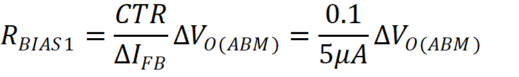
- RBIAS1 is determined based on a given current transfer ratio (CTR) of the optocoupler, ΔVO(ABM), and target 4~5 μA of ΔIFB as example. At collector currents less than 100 μA, the CTR of most optocouplers can be as low as 10%, or 0.1 (used in this example), although some high performance devices can have higher CTR.
Equation 63.
- RINT selection is not designed for the small-signal compensation, but to resolve the slow large-signal response of the shunt regulator. Specifically, after a step-down load change from heavy load to no load occurs, the output voltage overshoot and the long settling time forces ATL431 to reduce the cathode voltage continuously by the integrator configuration until the output voltage gets back to normal regulation level. If the load step-up transient happens before the output voltage is settled from the previous load step-down event, the low voltage across ATL431 becomes the initial voltage level for the integrator to move to a new steady-state. Since the time for ATL431 to move from lower voltage to a high voltage delays iFB reduction, the controller response from SBP mode to AAM mode is delayed as well, which slows down the energy delivery to the output and results in a large voltage undershoot.
To resolve this problem, RINT behaves like a current-limiting resistor for CINT, which slows down the reduction of the cathode voltage of ATL431. RINT needs to be adjusted based on the voltage undershoot requirement under the highest repetitive rate of load change.