SLUSDK4E may 2020 – july 2023 UCC28782
PRODUCTION DATA
- 1
- 1 Features
- 2 Applications
- 3 Description
- 4 Revision History
- 5 Device Comparison Table
- 6 Pin Configuration and Functions
- 7 Specifications
-
8 Detailed Description
- 8.1 Overview
- 8.2 Functional Block Diagram
- 8.3
Detailed Pin Description
- 8.3.1 BUR Pin (Programmable Burst Mode)
- 8.3.2 FB Pin (Feedback Pin)
- 8.3.3 REF Pin (Internal 5-V Bias)
- 8.3.4 VDD Pin (Device Bias Supply)
- 8.3.5 P13 and SWS Pins
- 8.3.6 S13 Pin
- 8.3.7 IPC Pin (Intelligent Power Control Pin)
- 8.3.8 RUN Pin (Driver and Bias Source for Isolator)
- 8.3.9 PWMH and AGND Pins
- 8.3.10 PWML and PGND Pins
- 8.3.11 SET Pin
- 8.3.12 RTZ Pin (Sets Delay for Transition Time to Zero)
- 8.3.13 RDM Pin (Sets Synthesized Demagnetization Time for ZVS Tuning)
- 8.3.14 BIN, BSW, and BGND Pins
- 8.3.15 XCD Pin
- 8.3.16 CS, VS, and FLT Pins
- 8.4
Device Functional Modes
- 8.4.1 Adaptive ZVS Control with Auto-Tuning
- 8.4.2 Dead-Time Optimization
- 8.4.3 EMI Dither and Dither Fading Function
- 8.4.4 Control Law across Entire Load Range
- 8.4.5 Adaptive Amplitude Modulation (AAM)
- 8.4.6 Adaptive Burst Mode (ABM)
- 8.4.7 Low Power Mode (LPM)
- 8.4.8 First Standby Power Mode (SBP1)
- 8.4.9 Second Standby Power Mode (SBP2)
- 8.4.10 Startup Sequence
- 8.4.11 Survival Mode of VDD (INT_STOP)
- 8.4.12 Capacitor Voltage Balancing Function
- 8.4.13 Device Functional Modes for Bias Regulator Control
- 8.4.14
System Fault Protections
- 8.4.14.1 Brown-In and Brown-Out
- 8.4.14.2 Output Over-Voltage Protection (OVP)
- 8.4.14.3 Input Over Voltage Protection (IOVP)
- 8.4.14.4 Over-Temperature Protection (OTP) on FLT Pin
- 8.4.14.5 Over-Temperature Protection (OTP) on CS Pin
- 8.4.14.6 Programmable Over-Power Protection (OPP)
- 8.4.14.7 Peak Power Limit (PPL)
- 8.4.14.8 Output Short-Circuit Protection (SCP)
- 8.4.14.9 Over-Current Protection (OCP)
- 8.4.14.10 External Shutdown
- 8.4.14.11 Internal Thermal Shutdown
- 8.4.15 Pin Open/Short Protections
-
9 Application and Implementation
- 9.1 Application Information
- 9.2
Typical Application Circuit
- 9.2.1 Design Requirements for a 65-W USB-PD Adapter Application
- 9.2.2
Detailed Design Procedure
- 9.2.2.1 Input Bulk Capacitance and Minimum Bulk Voltage
- 9.2.2.2 Transformer Calculations
- 9.2.2.3 Clamp Capacitor Calculation
- 9.2.2.4 Bleed-Resistor Calculation
- 9.2.2.5 Output Filter Calculation
- 9.2.2.6 Calculation of ZVS Sensing Network
- 9.2.2.7 Calculation of BUR Pin Resistances
- 9.2.2.8 Calculation of Compensation Network
- 9.2.3 Application Curves
- 10Power Supply Recommendations
- 11Layout
- 12Device and Documentation Support
- 13Mechanical, Packaging, and Orderable Information
Package Options
Mechanical Data (Package|Pins)
- RTW|24
Thermal pad, mechanical data (Package|Pins)
- RTW|24
Orderable Information
9.2.2.6 Calculation of ZVS Sensing Network
There are three components in the application circuit to help the depletion MOSFET (QS) perform ZVS sensing safely: CSWS, RSWS, and DSWS. Design considerations and selection guidelines for the values of these components are given here.
At the rising edge of the switch node voltage, the fast dV/dt coupling through the drain-to-source capacitance of QS (COSS(Qs)) generates a charge current flowing into the circuit loading on the QS source pin. The result is a possible voltage overshoot on both the SWS pin and across the gate-to-source of QS (VGS(Qs)) since the gate is tied to P13. The SWS pin, with an absolute maximum voltage rating of 38 V, can handle higher voltage stress than VGS(Qs). Therefore, a capacitor (CSWS) between the SWS pin and GND should be selected properly to prevent the voltage overshoot from damaging the QS gate. Since COSS(Qs) and CSWS form a voltage divider, the minimum CSWS (CSWS(MIN)) can be derived as
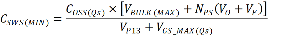
where VGS_MAX(Qs) is the de-rated maximum gate-to-source voltage of QS and VP13 is the steady-state voltage level of 13 V.
Without resistive damping, both the charge current on the rising edge of VSW and the discharge current on the falling edge of VSW are oscillatory with the parasitic series inductance within the ZVS sensing network resonating with CSWS. Therefore, a series resistor (RSWS) between SWS pin and source-pin of QS is used to dampen any high-frequency ringing, helping to obtain a cleaner sensing signal on the SWS pin and preventing any high-frequency current from interfering with other noise-sensitive signals. RSWS can be expressed as:
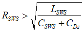
where LSWS is the lumped parasitic inductance including the packaging of QS and PCB traces of QS and CSWS return path.
A bidirectional TVS across BSS126 gate and source should be added to protect the gate-to-source voltage from potential abnormal voltage stress. The clamping voltage of TVS should be less than BSS126 voltage rating but greater than 15 V. The resistor should be slightly higher than 500 Ω. The resistor and a 22-pF ceramic capacitor between the SWS pin and the bulk input capacitor ground form a small sensing delay to help the internal detection circuit to identify the ZVS characteristic correctly.
Based on the above design guide, even though RSWS and CSWS may be sufficient to manage the voltage overshoot in normal operation, a low-capacitance bi-directional TVS diode (DSWS) across BSS126 gate and source is highly recommended to serve as a safety backup of the ZVS sensing network. Regular Zener diodes are not suitable due to high capacitance and slow clamping response. The clamping voltage of TVS should be less than BSS126 voltage rating but greater than 15 V.
A general recommendation is to use a 50-V 22-pF C0G-type ceramic capacitor for CSWS, a 510-Ω chip resistor for RSWS, and a bi-directional TVS diode with clamp voltage of 18 V for DSWS. Too large of RSWS or CSWS introduces a sensing delay between the actual VSW and the SWS pin, causing the ZVS control to unnecessarily extend tDM in order to pull down VSW earlier than expected before the end of tZ . As shown in Figure 8-5, the larger RSWS is, the smaller supply current to charge the VDD capacitor. If the reduced charge current (ISWS) is lower than the total consumed current from the controller (ISTART) and from the external circuitry on the VDD pin and P13 pin, VVDD may not be able to reach VVDD(ON) and the controller can not initiate any switching event.