SLUSA16D March 2010 – November 2016 UCC28950
PRODUCTION DATA.
- 1 Features
- 2 Applications
- 3 Description
- 4 Revision History
- 5 Pin Configuration and Functions
- 6 Specifications
-
7 Detailed Description
- 7.1 Overview
- 7.2 Functional Block Diagram
- 7.3
Feature Description
- 7.3.1 Start-Up Protection Logic
- 7.3.2 Voltage Reference (VREF)
- 7.3.3 Error Amplifier (EA+, EA-, COMP)
- 7.3.4 Soft Start and Enable (SS/EN)
- 7.3.5 Light-Load Power Saving Features
- 7.3.6 Adaptive Delay, (Delay between OUTA and OUTB, OUTC and OUTD (DELAB, DELCD, ADEL))
- 7.3.7 Adaptive Delay (Delay between OUTA and OUTF, OUTB and OUTE (DELEF, ADELEF))
- 7.3.8 Minimum Pulse (TMIN)
- 7.3.9 Burst Mode
- 7.3.10 Switching Frequency Setting
- 7.3.11 Slope Compensation (RSUM)
- 7.3.12 Dynamic SR ON/OFF Control (DCM Mode)
- 7.3.13 Current Sensing (CS)
- 7.3.14 Cycle-by-Cycle Current Limit Current Protection and Hiccup Mode
- 7.3.15 Synchronization (SYNC)
- 7.3.16 Outputs (OUTA, OUTB, OUTC, OUTD, OUTE, OUTF)
- 7.3.17 Supply Voltage (VDD)
- 7.3.18 Ground (GND)
- 7.4 Device Functional Modes
-
8 Application and Implementation
- 8.1 Application Information
- 8.2
Typical Application
- 8.2.1 Design Requirements
- 8.2.2
Detailed Design Procedure
- 8.2.2.1 Power Loss Budget
- 8.2.2.2 Preliminary Transformer Calculations (T1)
- 8.2.2.3 QA, QB, QC, QD FET Selection
- 8.2.2.4 Selecting LS
- 8.2.2.5 Selecting Diodes DB and DC
- 8.2.2.6 Output Inductor Selection (LOUT)
- 8.2.2.7 Output Capacitance (COUT)
- 8.2.2.8 Select FETs QE and QF
- 8.2.2.9 Input Capacitance (CIN)
- 8.2.2.10 Current Sense Network (CT, RCS, R7, DA)
- 8.2.3 Application Curves
- 9 Power Supply Recommendations
- 10Layout
- 11Device and Documentation Support
- 12Mechanical, Packaging, and Orderable Information
Package Options
Mechanical Data (Package|Pins)
- PW|24
Thermal pad, mechanical data (Package|Pins)
Orderable Information
8 Application and Implementation
NOTE
Information in the following applications sections is not part of the TI component specification, and TI does not warrant its accuracy or completeness. TI’s customers are responsible for determining suitability of components for their purposes. Customers should validate and test their design implementation to confirm system functionality.
8.1 Application Information
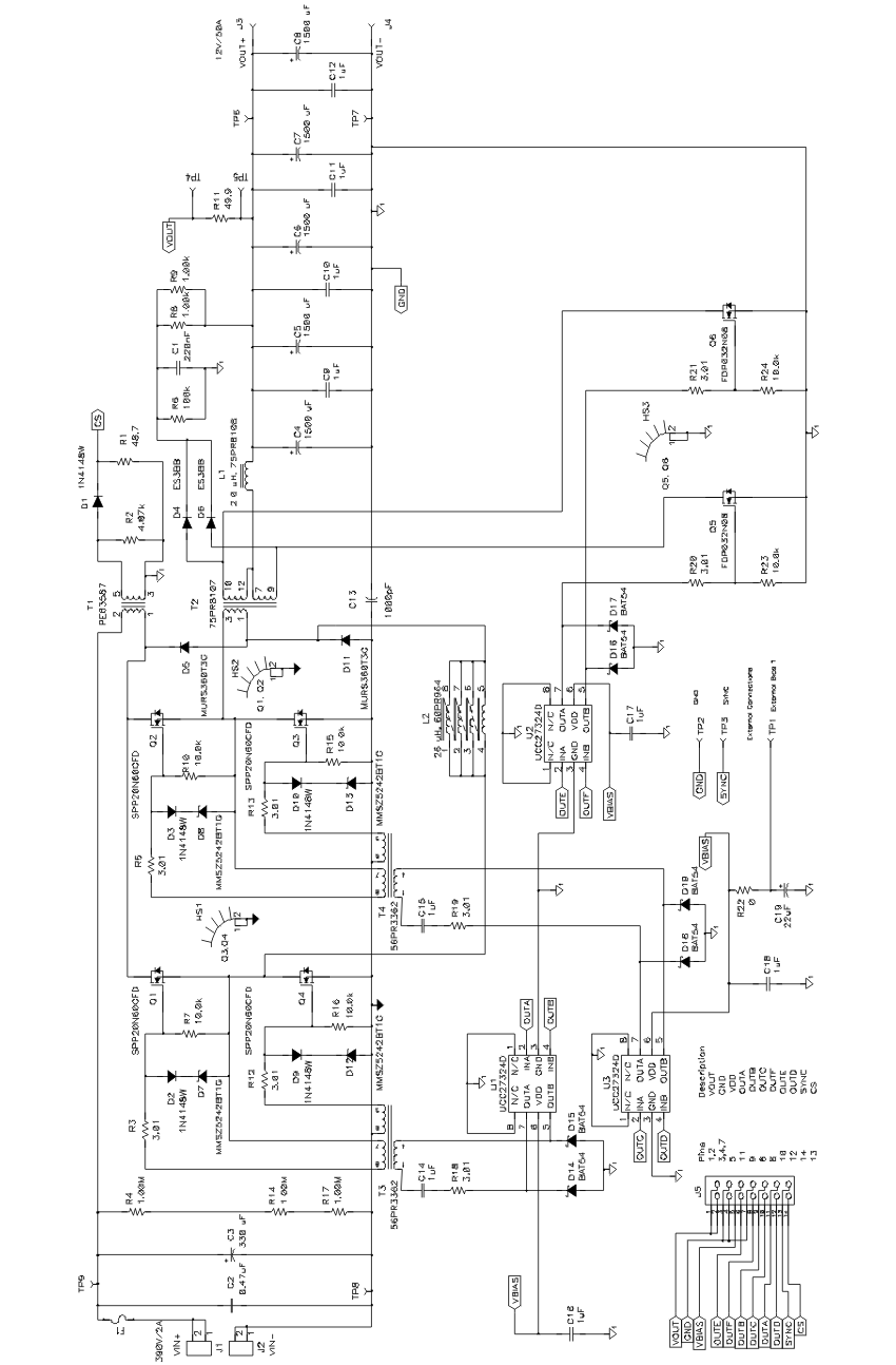
The high efficiency of a phase-shifted full-bridge DC/DC converter using the UCC28950 is achieved by using synchronous rectification, a control algorithm providing ZVS condition over the entire load current range, accurate adaptive timing of the control signals between primary and secondary FETs and special operating modes at light load. A simplified electrical diagram of this converter is shown in Figure 48. The controller device is located on the secondary side of converter, although it could be located on primary side as well. The location on secondary side allows easy power system level communication and better handling of some transient conditions that require fast direct control of the synchronous rectifier MOSFETs. The power stage includes primary side MOSFETs, QA, QB, QC, QD and secondary side synchronous rectifier MOSFETs, QE and QF. For example, for the 12-V output converters in server power supplies use of the center-tapped rectifier scheme with L-C output filter is a popular choice.
To maintain high efficiency at different output power conditions, the converter operates in synchronous rectification mode at mid and high output power levels, transitioning to diode rectifier mode at light load and then into burst mode as the output power becomes even lower. All these transitions are based on current sensing on the primary side using a current sense transformer in this specific case.
The major waveforms of the phase-shifted converter during normal operation are shown in Figure 46. The upper six waveforms in Figure 46 show the output drive signals of the controller. In normal mode, the outputs OUTE and OUTF overlap during the part of the switching cycle when both rectifier MOSFETs are conducting and the windings of the power transformer are shorted. Current, IPR, is the current flowing through the primary winding of the power transformer. The bottom four waveforms show the drain-source voltages of rectifier MOSFETs, VDS_QE and VDS_QF, the voltage at the output inductor, V LOUT, and the current through the output inductor, I LOUT. Proper timing between the primary switches and synchronous rectifier MOSFETs is critical to achieve highest efficiency and reliable operation in this mode. The controller device adjusts the turn OFF timing of the rectifier MOSFETs as a function of load current to ensure minimum conduction time and reverse recovery losses of their internal body diodes.
ZVS is an important feature of relatively high input voltage converters in reducing switching losses associated with the internal parasitic capacitances of power switches and transformers. The controller ensures ZVS conditions over the entire load current range by adjusting the delay time between the primary MOSFETs switching in the same leg in accordance to the load variation. The controller also limits the minimum ON-time pulse applied to the power transformer at light load, allowing the storage of sufficient energy in the inductive components of the power stage for the ZVS transition.
As the load current reduces from full load down to the no-load condition, the controller selects the most efficient power saving mode by moving from the normal operation mode to the discontinuous-current diode-rectification mode and, eventually, at very light-load and at no-load condition, to the burst mode. These modes and related output signals, OUTE, OUTF, driving the rectifier MOSFETs, are shown in Figure 47.
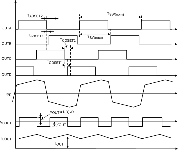 Figure 46. Major Waveforms of Phase-Shifted Converter
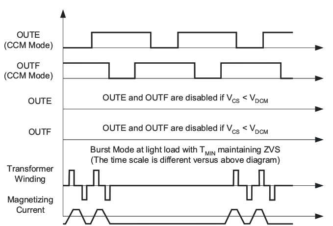 Figure 47. Major Waveforms During Transitions Between Different Operating Modes
It is necessary to prevent the reverse current flow through the synchronous rectifier MOSFETs and output inductor at light load, during parallel operation and at some transient conditions. Such reverse current results in circulating of some extra energy between the input voltage source and the load and, therefore, causes increased losses and reduced efficiency. Another negative effect of such reverse current is the loss of ZVS condition. The suggested control algorithm prevents reverse current flow, still maintaining most of the benefits of synchronous rectification by switching off the drive signals of rectifier MOSFETs in a predetermined way. At some pre-determined load current threshold, the controller disables outputs OUTE and OUTF by bringing them down to zero.
Synchronous rectification using MOSFETs requires some electrical energy to drive the MOSFETs. There is a condition below some light-load threshold when the MOSFET drive related losses exceed the saving provided by the synchronous rectification. At such light load, it is best to disable the drive circuit and use the internal body diodes of rectifier MOSFETs, or external diodes in parallel with the MOSFETs, for more efficient rectification. In most practical cases, the drive circuit needs to be disabled close to DCM mode. This mode of operation is called discontinuous-current diode-rectification mode.
At very light-load and no-load condition, the duty cycle, demanded by the closed-feedback-loop control circuit for output voltage regulation, can be very low. This could lead to the loss of ZVS condition and increased switching losses. To avoid the loss of ZVS, the control circuit limits the minimum ON-time pulse applied to the power transformer using resistor from TMIN pin to GND. Therefore, the only way to maintain regulation at very light load and at no-load condition is to skip some pulses. The controller skips pulses in a controllable manner to avoid saturation of the power transformer. Such operation is called burst mode. In Burst Mode there are always an even number of pulses applied to the power transformer before the skipping off time. Thus, the flux in the core of the power transformer always starts from the same point during the start of every burst of pulses.
8.2 Typical Application
A typical application for the UCC28950 device is a controller for a phase-shifted full-bridge converter that converts a 390-VDC input to a regulated 12-V output using synchronous rectifiers to achieve high efficiency.
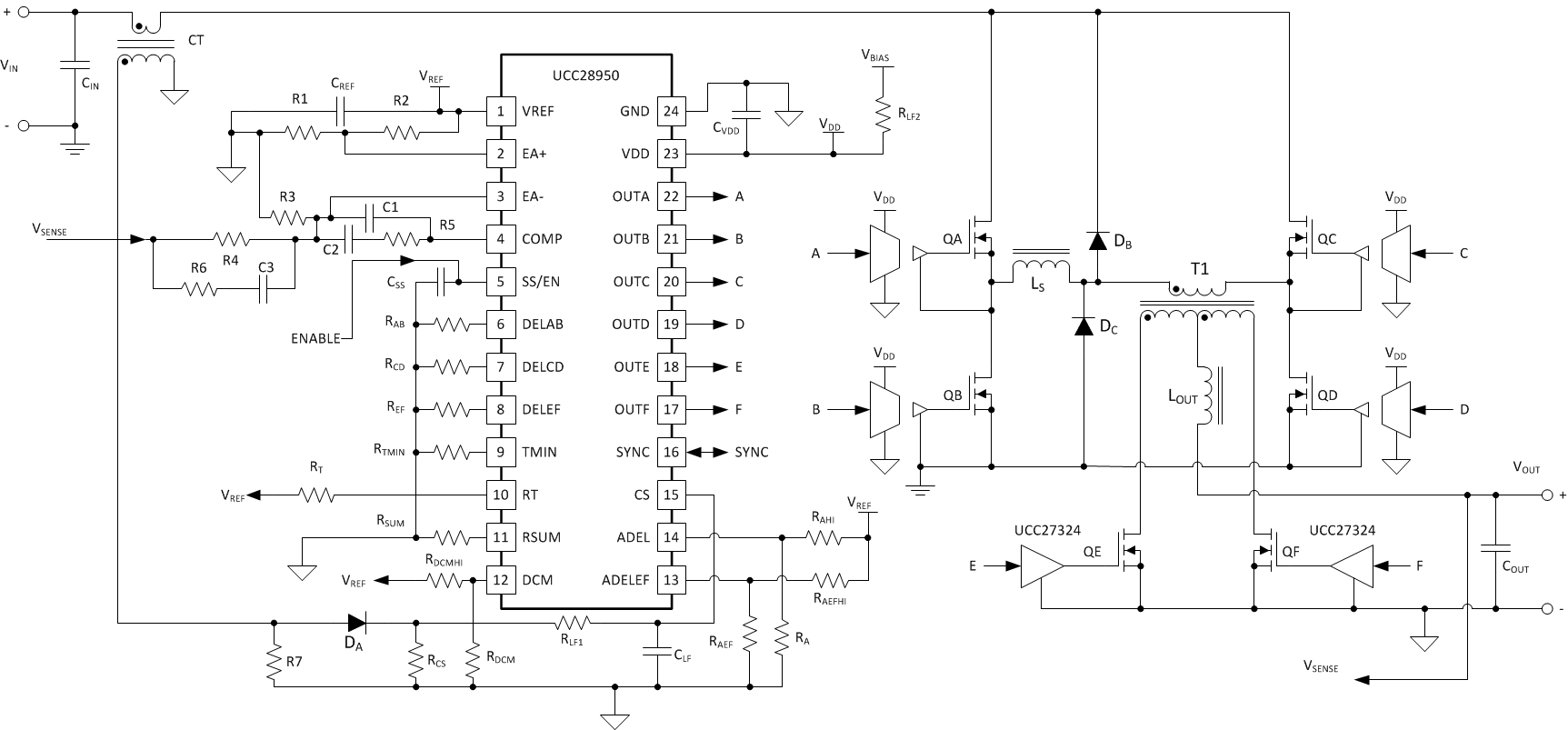 Figure 48. UCC28950 Typical Application
8.2.1 Design Requirements
Table 1 lists the requirements for this application.
Table 1. UCC28950 Typical Application Design Requirements
| PARAMETER | TEST CONDITIONS | MIN | TYP | MAX | UNIT | |
|---|---|---|---|---|---|---|
| INPUT CHARACTERISTICS | ||||||
| VIN | DC input voltage range | 370 | 390 | 410 | V | |
| IIN(max) | Maximum input current | VIN= 370 VDC to 410 VDC | 2 | A | ||
| OUTPUT CHARACTERISTICS | ||||||
| VOUT | Output voltage | VIN= 370 VDC to 410 VDC | 11.4 | 12 | 12.6 | V |
| IOUT | Output current | VIN= 370 VDC to 410 VDC | 50 | A | ||
| Output voltage transient | 90% load step | 600 | mV | |||
| POUT | Continuous output power | VIN= 370 VDC to 410 VDC | 600 | W | ||
| Load regulation | VIN = 370 VDC to 410 VDC, IOUT= 5 A to 50 A | 140 | mV | |||
| Line regulation | VIN = 370 VDC to 410 VDC, IOUT= 5 A to 50 A | 140 | mV | |||
| Output ripple voltage | VIN = 370 VDC to 410 VDC, IOUT= 5 A to 50 A | 200 | mV | |||
| SYSTEM | ||||||
| FSW | Switching Frequency | 100 | kHz | |||
| Full-load efficiency | VIN= 370 VDC to 410 VDC, POUT= 500 W | 93% | 94% | |||
8.2.2 Detailed Design Procedure
In high-power server applications to meet high-efficiency and green standards some power-supply designers have found it easier to use a phase-shifted, full-bridge converter. This is because the phase-shifted, full-bridge converter can obtain zero-voltage switching on the primary side of the converter, reducing switching losses, and EMI and increasing overall efficiency.
This is a review of the design of a 600-W, phase-shifted, full-bridge converter for one of these power systems using TI's UCC28950 device, which is based on typical values. In a production design, the values may need to be modified for worst-case conditions. TI has provided a MathCAD Design Tool and an Excel Design Tool to support the system designer. Both tools can be accessed in the Tools and Software tab of the UCC28950 product folder on TI.com, or can be downloaded through the following links: MathCAD Design Tool, Excel Design Tool.
NOTE
FSW refers to the switching frequency applied to the power transformer. The output inductor experiences a switching frequency which is 2 x FSW .
8.2.2.1 Power Loss Budget
To meet the efficiency goal a power loss budget needs to be set.

8.2.2.2 Preliminary Transformer Calculations (T1)
Transformer turns ratio (a1):

Estimated FET voltage drop (VRDSON):

Select transformer turns based on 70% duty cycle (DMAX) at minimum specified input voltage. This will give some room for dropout if a PFC front end is used.


Turns ratio rounded to the nearest whole turn.

Calculated typical duty cycle (DTYP) based on average input voltage.

Output inductor peak-to-peak ripple current is set to 20% of the output current.

Care must be taken in selecting the correct amount of magnetizing inductance (LMAG). The following equations calculate the minimum magnetizing inductance of the primary of the transformer (T1) to ensure the converter operates in current-mode control. As LMAG reduces, the increasing magnetizing current becomes an increasing proportion of the signal at the CS pin. If the magnetizing current increases enough it can swamp out the current sense signal across RCS and the converter will operate increasingly as if it were in voltage mode control rather than current mode.

Figure 49 shows T1 primary current (IPRIMARY) and synchronous rectifiers QE (IQE) and QF (IQF) currents with respect to the synchronous rectifier gate drive currents. Note that IQE and IQF are the same as the secondary winding currents of T1. Variable D is the duty cycle of the converter.
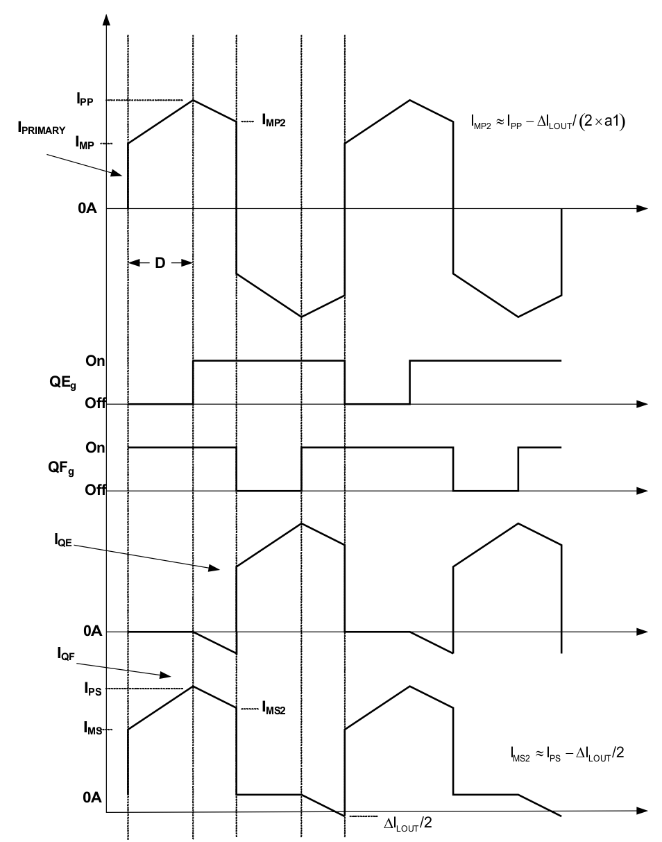 Figure 49. T1 Primary and QE and QF FET Currents
Calculate T1 secondary RMS current (ISRMS):


Secondary RMS current (ISRMS1) when energy is being delivered to the secondary:

Secondary RMS current (ISRMS2) when current is circulating through the transformer when QE and QF are both on.

Secondary RMS current (ISRMS3) caused by the negative current in the opposing winding during freewheeling period, please refer to Figure 49.

Total secondary RMS current (ISRMS):

Calculate T1 Primary RMS Current (IPRMS):


T1 Primary RMS (IPRMS1) current when energy is being delivered to the secondary.

T1 Primary RMS (IPRMS2) current when the converter is free wheeling.

Total T1 primary RMS current (IPRMS):

For this design a Vitec™ transformer was selected part number 75PR8107 that had the following specifications.


Measure leakage inductance on the Primary:

Transformer Primary DC resistance:

Transformer Secondary DC resistance:

Estimated transformer core losses (PT1) are twice the copper loss.
NOTE
This is just an estimate and the total losses may vary based on magnetic design.

Calculate remaining power budget:

8.2.2.3 QA, QB, QC, QD FET Selection
In this design to meet efficiency and voltage requirements 20 A, 650 V, CoolMOS FETs from Infineon are chosen for QA..QD.
FET drain to source on resistance:

FET Specified COSS:

Voltage across drain-to-source (VdsQA) where COSS was measured, data sheet parameter:

Calculate average Coss [2]:

QA FET gate charge:

Voltage applied to FET gate to activate FET:

Calculate QA losses (PQA) based on Rds(on)QA and gate charge (QAg):

Recalculate power budget:

8.2.2.4 Selecting LS
Calculating the value of the shim inductor (LS) is based on the amount of energy required to achieve zero voltage switching. This inductor needs to able to deplete the energy from the parasitic capacitance at the switch node. The following equation selects LS to achieve ZVS at 100% load down to 50% load based on the primary FET’s average total COSS at the switch node.
NOTE
The actual parasitic capacitance at the switched node may differ from the estimate and LS may have to be adjusted accordingly.

For this design a 26-µH Vitec inductor was chosen for LS, part number 60PR964. The shim inductor had the following specifications.

LS DC Resistance:

Estimate LS power loss (PLS) and readjust remaining power budget:


8.2.2.5 Selecting Diodes DB and DC
There is a potential for high voltage ringing on the secondary rectifiers, caused by the difference in current between the transformer and the shim inductor when the transformer comes out of freewheeling. Diodes DB and DC provide a path for this current and prevent any ringing by clamping the transformer primary to the primary side power rails. Normally these diodes do not dissipate much power but they should be sized to carry the full primary current. The worse case power dissipated in these diodes is:

The diodes should be ultra-fast types and rated for the input voltage of the converter – VIN (410 VDC in this case).
A MURS360 part is suitable at this power level.
8.2.2.6 Output Inductor Selection (LOUT)
Inductor LOUT is designed for 20% inductor ripple current (∆ILOUT):


Calculate output inductor RMS current (ILOUT_RMS):

A 2-µH inductor from Vitec Electronics Corporation, part number 75PR8108, is suitable for this design. The inductor has the following specifications.

Output inductor DC resistance:

Estimate output inductor losses (PLOUT) and recalculate power budget. Note PLOUT is an estimate of inductor losses that is twice the copper loss. Note this may vary based on magnetic manufactures. It is advisable to double check the magnetic loss with the magnetic manufacture.


8.2.2.7 Output Capacitance (COUT)
The output capacitor is selected based on holdup and transient (VTRAN) load requirements.
Time it takes LOUT to change 90% of its full load current:

During load transients most of the current will immediately go through the capacitors equivalent series resistance (ESRCOUT). The following equations are used to select ESRCOUT and COUT based on a 90% load step in current. The ESR is selected for 90% of the allowable transient voltage (VTRAN), while the output capacitance (COUT) is selected for 10% of VTRAN.


Before selecting the output capacitor, the output capacitor RMS current (ICOUT_RMS) must be calculated.

To meet the design requirements five 1500-µF, aluminum electrolytic capacitors are chosen for the design from United Chemi-Con™, part number EKY-160ELL152MJ30S. These capacitors have an ESR of 31 mΩ.
Number of output capacitors:

Total output capacitance:

Effective output capacitance ESR:

Calculate output capacitor loss (PCOUT):

Recalculate remaining Power Budget:

8.2.2.8 Select FETs QE and QF
Selecting FETs for a design is an iterative process. To meet the power requirements of this design, we select 75-V, 120-A FETs, from Fairchild, part number FDP032N08. These FETs have the following characteristics.


Calculate average FET COSS (COSS_QE_AVG) based on the data sheet parameters for COSS (COSS_SPEC), and drain to source voltage where COSS_SPEC was measured (Vds_spec), and the maximum drain to source voltage in the design (VdsQE) that will be applied to the FET in the application.
Voltage across FET QE and QF when they are off:

Voltage where FET COSS is specified and tested in the FET data sheet:

Specified output capacitance from FET data sheet:

Average QE and QF COSS [2]:

QE and QF RMS current:

To estimate FET switching loss the Vg vs. Qg curve from the FET data sheet needs to be studied. First the gate charge at the beginning of the miller plateau needs to be determined (QEMILLER_MIN) and the gate charge at the end of the miller plateau (QEMILLER_MAX) for the given VDS.
Maximum gate charge at the end of the miller plateau:

Minimum gate charge at the beginning of the miller plateau:

NOTE
The FETs in this design are driven with a UCC27324 Gate Driver IC, setup to drive 4-A (IP) of gate drive current.

Estimated FET Vds rise and fall time:

Estimate QE and QF FET Losses (PQE):


Recalculate the power budget.

8.2.2.9 Input Capacitance (CIN)
The input voltage in this design is 390 VDC, which is generally fed by the output of a PFC boost pre-regulator. The input capacitance is generally selected based on holdup and ripple requirements.
NOTE
The delay time needed to achieve ZVS can act as a duty cycle clamp (DCLAMP).
Calculate tank frequency:

Estimated delay time:

Effective duty cycle clamp (DCLAMP):

VDROP is the minimum input voltage where the converter can still maintain output regulation. The converter’s input voltage would only drop down this low during a brownout or line-drop condition if this converter was following a PFC pre-regulator.

CIN was calculated based on one line cycle of holdup:

Calculate high frequency input capacitor RMS current (ICINRMS).

To meet the input capacitance and RMS current requirements for this design a 330-µF capacitor was chosen from Panasonic part number EETHC2W331EA.

This capacitor has a high frequency (ESRCIN) of 150 mΩ, measured with an impedance analyzer at 200 kHz.

Estimate CIN power dissipation (PCIN):

Recalculate remaining power budget:

There is roughly 6.0 W left in the power budget left for the current sensing network, and biasing the control device and all resistors supporting the control device.
8.2.2.10 Current Sense Network (CT, RCS, R7, DA)
The CT chosen for this design has a turns ratio (CTRAT) of 100:1

Calculate nominal peak current (IP1) at VINMIN:
Peak primary current:

The CS pin voltage where peak current limit will trip.

Calculate current sense resistor (RCS) and leave 300mV for slope compensation. Include a 1.1 factor for margin:

Select a standard resistor for RCS:

Estimate power loss for RCS:

Calculate maximum reverse voltage (VDA) on DA:

Estimate DA power loss (PDA):

Calculate reset resistor R7:
Resistor R7 is used to reset the current sense transformer CT.

Resistor RLF1 and capacitor CLF form a low pass filter for the current sense signal (Pin 15). For this design we chose the following values. This filter has a low frequency pole (fLFP) at 482 kHz. This should work for most applications but may be adjusted to suit individual layouts and EMI present in the design.


The UCC28950 VREF output (Pin 1) needs a high frequency bypass capacitor to filter out high frequency noise. This pin needs at least 1 µF of high frequency bypass capacitance (CREF).

The voltage amplifier reference voltage (Pin 2, EA +) can be set with a voltage divider (R1, R2), for this design example, the error amplifier reference voltage (V1) will be set to 2.5 V. Select a standard resistor value for R1 and then calculate resistor value R2.
UCC28950 reference voltage:

Set voltage amplifier reference voltage:


Voltage divider formed by resistor R3 and R4 are chosen to set the DC output voltage (VOUT) at Pin 3 (EA-).
Select a standard resistor for R3:

Calculate R4:

Then choose a standard resistor for R4:

8.2.2.10.1 Voltage Loop Compensation Recommendation
For best results in the voltage loop, TI recommends using a Type 2 or Type 3 compensation network (Figure 50). A Type 2 compensation network does not require passive components CZ2 and RZ2. Type 1 compensation is not versatile enough for a phase shifted full bridge. When evaluating the COMP for best results, TI recommends placing a 1-kΩ resistor between the socpe probe and the COMP pin of the UCC28950.
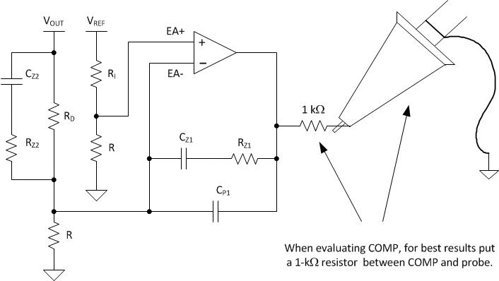 Figure 50. Type 3 Compensation Evaluation
Compensating the feedback loop can be accomplished by properly selecting the feedback components (R5, C1 and C2). These components are placed as close as possible to pin 3 and 4 of the UCC28950. A Type 2 compensation network is designed in this example.
Calculate load impedance at 10% load (RLOAD):

Approximation of control to output transfer function (GCO(f)) as a function of frequency:

Double pole frequency of GCO(f):

Angular velocity:

Compensate the voltage loop with type 2 feedback network. The following transfer function is the compensation gain as a function of frequency (GC(f)).

Calculate voltage loop feedback resistor (R5) based on crossing the voltage loop (fC) over at a 10th of the double pole frequency (fPP).


Select a standard resistor for R5.

Calculate the feedback capacitor (C2) to give added phase at crossover.

Select a standard capacitance value for the design.

Put a pole at two times fC.

Select a standard capacitance value for the design.

Loop gain as a function of frequency (TV(f)) in dB.

Plot theoretical loop gain and phase to graphically check for loop stability (Figure 51). The theoretical loop gain crosses over at roughly 3.7 kHz with a phase margin of greater than 90 degrees.
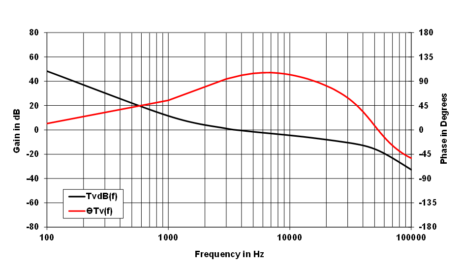 Figure 51. Loop Gain and Phase vs Frequency
NOTE
TI recommends checking your loop stability of your final design with transient testing and/or a network analyzer and adjust the compensation (GC(f)) feedback as necessary.

where
- Loop Gain (TVdB(f)), Loop Phase (ΦTV(f))
To limit over shoot during power up the UCC28950 has a soft-start function (SS, Pin 5) which in this application was set for a soft start time of 15 ms (tSS).


Select a standard capacitor for the design.

This application note presents a fixed delay approach to achieving ZVS from 100% load down to 50% load. Adaptive delays can be generated by connecting the ADEL and ADELEF pins to the CS pin as shown in Figure 52.
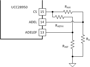 Figure 52. UCC28950 Adaptive Delays
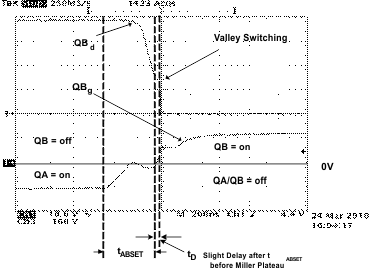
When the converter is operating below 50% load the converter will be operating in valley switching. In order to achieve zero voltage switching on switch node of QBd, the turn-on (tABSET) delays of FETs QA and QB need to be initially set based on the interaction of LS and the theoretical switch node capacitance. The following equations are used to set tABSET initially.
Equate shim inductance to two times COSS capacitance:

Calculate tank frequency:

Set initial tABSET delay time and adjust as necessary.
NOTE
The 2.25 factor of the tABSET equation was derived from empirical test data and may vary based on individual design differences.

The resistor divider formed by RA and RAHI programs the tABSET, tCDSET delay range of the UCC28950. Select a standard resistor value for RAHI.
NOTE
tABSET can be programmed between 30 ns to 1000 ns.

The voltage at the ADEL input of the UCC28950 (VADEL) needs to be set with RA based on the following conditions.
If tABSET > 155 ns set VADEL = 0.2 V, tABSET can be programmed between 155 ns and 1000 ns:
If tABSET ≤ 155 ns set VADEL = 1.8 V, tABSET can be programmed between 29 ns and 155 ns:
Based on VADEL selection, calculate RA:

Select the closest standard resistor value for RA:

Recalculate VADEL based on resistor divider selection:

Resistor RAB programs tABSET:

Select a standard resistor value for the design:

NOTE
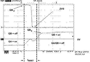
Once you have a prototype up and running it is recommended you fine tune tABSET at light load to the peak and valley of the resonance between LS and the switch node capacitance. In this design the delay was set at 10% load. Please refer to Figure 53.
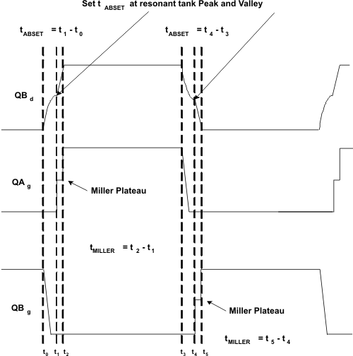 Figure 53. tABSET to Achieve Valley Switching at Light Loads
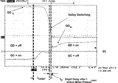
The QC and QD turnon delays (tCDSET) should be initially set for the same delay as the QA and QB turn on delays (Pin 6). The following equations program the QC and QD turn-on delays (tCDSET) by properly selecting resistor RDELCD (Pin 7).

Resistor RCD programs tCDSET:

Select a standard resistor for the design:

NOTE
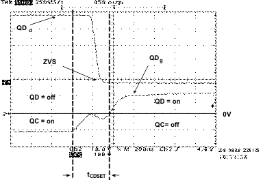
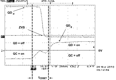
Once you have a prototype up and running it is recommended to fine tune tCDSET at light load. In this design the CD node was set to valley switch at roughly 10% load. Please refer to Figure 54. Obtaining ZVS at lighter loads with switch node QDd is easier due to the reflected output current present in the primary of the transformer at FET QD and QC turnoff/on. This is because there was more peak current available to energize LS before this transition, compared to the QA and QB turnoff/on.
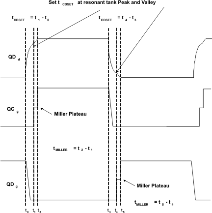 Figure 54. tCDSET to Achieve Valley Switching at Light Loads
There is a programmable delay for the turnoff of FET QF after FET QA turnoff (tAFSET) and the turnoff of FET QE after FET QB turnoff (tBESET). A good place to set these delays is 50% of tABSET. This will ensure that the appropriate synchronous rectifier turns off before the AB ZVS transition. If this delay is too large it will cause OUTE and OUTF not to overlap correctly and it will create excess body diode conduction on FETs QE and QF.

The resistor divider formed by RAEF and RAEFHI programs the tAFSET and tBESET delay range of the UCC28950. Select a standard resistor value for RAEFHI.
NOTE
tEFSET and tBESET can be programmed between 32 ns to 1100 ns.

The voltage at the ADELEF pin of the UCC28950 (VADELEF) needs to be set with RAEF based on the following conditions.
If tAFSET < 170 ns set VADEL = 0.2 V, tABSET can be programmed between 32 ns and 170 ns:
If tABSET > or = 170 ns set VADEL = 1.7 V, tABSET can be programmed between 170 ns and 1100 ns:
Based on VADELEF selection, calculate RAEF:

Select the closest standard resistor value for RAEF:

Recalculate VADELEF based on resistor divider selection:

The following equation was used to program tAFSET and tBESET by properly selecting resistor REF.

A standard resistor was chosen for the design.

Resistor RTMIN programs the minimum on time (tMIN) that the UCC28950 (Pin 9) can demand before entering burst mode. If the UCC28950 controller tries to demand a duty cycle on time of less than tMIN the power supply will go into burst mode operation. For this design we set the minimum on time to 75 ns.

The minimum on time is set by selecting RTMIN with the following equation.

A standard resistor value is then chosen for the design.

A resistor from the RT pin to ground sets the converter switching frequency.

Select a standard resistor for the design.

The UCC28950 provides slope compensation. The amount of slope compensation is set by the resistor RSUM. As suggested earlier, we set the slope compensation ramp to be half the inductor current ramp downslope (inductor current ramp during the off time), reflected through the main transformer and current sensing networks as explained earlier in Slope Compensation (RSUM).
The required slope compensation ramp is

The magnetizing current of the power transformer provides part of the compensating ramp and is calculated from Equation 169.

The required compensating ramp is

The value for the resistor, RSUM, may be found from the graph in Figure 37 or calculated from rearranged versions of Equation 12 or Equation 13 depending on whether the controller is operating in Current or Voltage Control Mode. In this case we are using Current Mode Control and Equation 12 is rearranged and evaluated as follows

Check that the 300mV we allowed for the slope compensation ramp when choosing RCS in Equation 110 is sufficient.

To increase efficiency at lighter loads the UCC28950 is programmed (Pin 12, DCM) under light load conditions to disable the synchronous FETs on the secondary side of the converter (QE and QF). This threshold is programmed with resistor divider formed by RDCMHI and RDCM. This DCM threshold needs to be set at a level before the inductor current goes discontinuous. The following equation sets the level at which the synchronous rectifiers are disabled at roughly 15% load current.

Select a standard resistor value for RDCM.

Calculate resistor value RDCMHI.

Select a standard resistor value for this design

NOTE
It is recommended to use an RCD clamp to protect the output synchronous FETs from overvoltage due to switch node ringing.
8.2.3 Application Curves
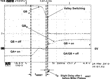
| VIN = 390 V | ||
| IOUT = 5 A |
and Primary Switch Nodes (QBd and QDd)
| VIN = 390 V | ||
| IOUT = 10 A |
and Switch Nodes (QBg QBd)
| VIN = 390 V | ||
| IOUT = 5 A |
and Primary Switch Nodes (QDg QDd)
| VIN = 390 V | ||
| IOUT = 10 A |
and Switch Nodes (QDg QDd)
NOTE
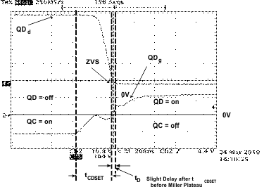
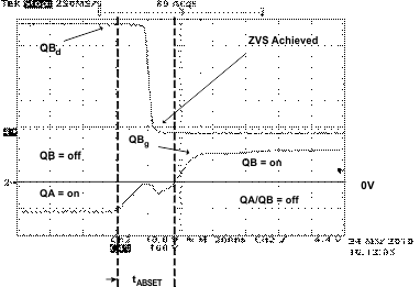
Switch node QBd is valley switching and node QDd has achieved ZVS. Please refer to Figure 59 and Figure 60. It is not uncommon for switch node QDd to obtain ZVS before QBd. This is because during the QDd switch node voltage transition, the reflected output current provides immediate energy for the LC tank at the switch node. Where at the QBd switch node transition the primary has been shorted out by the high side or low side FETs in the H bridge. This transition is dependent on the energy stored in LS and LLK to provide energy for the LC tank at switch node QBd making it take longer to achieve ZVS.
| VIN = 390 V | ||
| IOUT = 25 A |
and Switch Nodes (QBg QBd)
| VIN = 390 V | ||
| IOUT = 25 A |
and Switch Nodes (QDg QDd)
NOTE
When the converter is running at 25 A, both switch nodes are operating into zero voltage switching (ZVS). It is also worth mentioning that there is no evidence of the gate miller plateau during gate driver switching. This is because the voltage across the drains and sources of FETs QA through QD have already transitioned before.
| VIN = 390 V | ||
| IOUT = 50 A |
and Switch Nodes (QBg QBd)
| VIN = 390 V | ||
| IOUT = 50 A |
and Switch Nodes (QDg QDd)
NOTE
ZVS maintained from 50% to 100% output power.
