SLUSA16D March 2010 – November 2016 UCC28950
PRODUCTION DATA.
- 1 Features
- 2 Applications
- 3 Description
- 4 Revision History
- 5 Pin Configuration and Functions
- 6 Specifications
-
7 Detailed Description
- 7.1 Overview
- 7.2 Functional Block Diagram
- 7.3
Feature Description
- 7.3.1 Start-Up Protection Logic
- 7.3.2 Voltage Reference (VREF)
- 7.3.3 Error Amplifier (EA+, EA-, COMP)
- 7.3.4 Soft Start and Enable (SS/EN)
- 7.3.5 Light-Load Power Saving Features
- 7.3.6 Adaptive Delay, (Delay between OUTA and OUTB, OUTC and OUTD (DELAB, DELCD, ADEL))
- 7.3.7 Adaptive Delay (Delay between OUTA and OUTF, OUTB and OUTE (DELEF, ADELEF))
- 7.3.8 Minimum Pulse (TMIN)
- 7.3.9 Burst Mode
- 7.3.10 Switching Frequency Setting
- 7.3.11 Slope Compensation (RSUM)
- 7.3.12 Dynamic SR ON/OFF Control (DCM Mode)
- 7.3.13 Current Sensing (CS)
- 7.3.14 Cycle-by-Cycle Current Limit Current Protection and Hiccup Mode
- 7.3.15 Synchronization (SYNC)
- 7.3.16 Outputs (OUTA, OUTB, OUTC, OUTD, OUTE, OUTF)
- 7.3.17 Supply Voltage (VDD)
- 7.3.18 Ground (GND)
- 7.4 Device Functional Modes
-
8 Application and Implementation
- 8.1 Application Information
- 8.2
Typical Application
- 8.2.1 Design Requirements
- 8.2.2
Detailed Design Procedure
- 8.2.2.1 Power Loss Budget
- 8.2.2.2 Preliminary Transformer Calculations (T1)
- 8.2.2.3 QA, QB, QC, QD FET Selection
- 8.2.2.4 Selecting LS
- 8.2.2.5 Selecting Diodes DB and DC
- 8.2.2.6 Output Inductor Selection (LOUT)
- 8.2.2.7 Output Capacitance (COUT)
- 8.2.2.8 Select FETs QE and QF
- 8.2.2.9 Input Capacitance (CIN)
- 8.2.2.10 Current Sense Network (CT, RCS, R7, DA)
- 8.2.3 Application Curves
- 9 Power Supply Recommendations
- 10Layout
- 11Device and Documentation Support
- 12Mechanical, Packaging, and Orderable Information
Package Options
Mechanical Data (Package|Pins)
- PW|24
Thermal pad, mechanical data (Package|Pins)
Orderable Information
7 Detailed Description
7.1 Overview
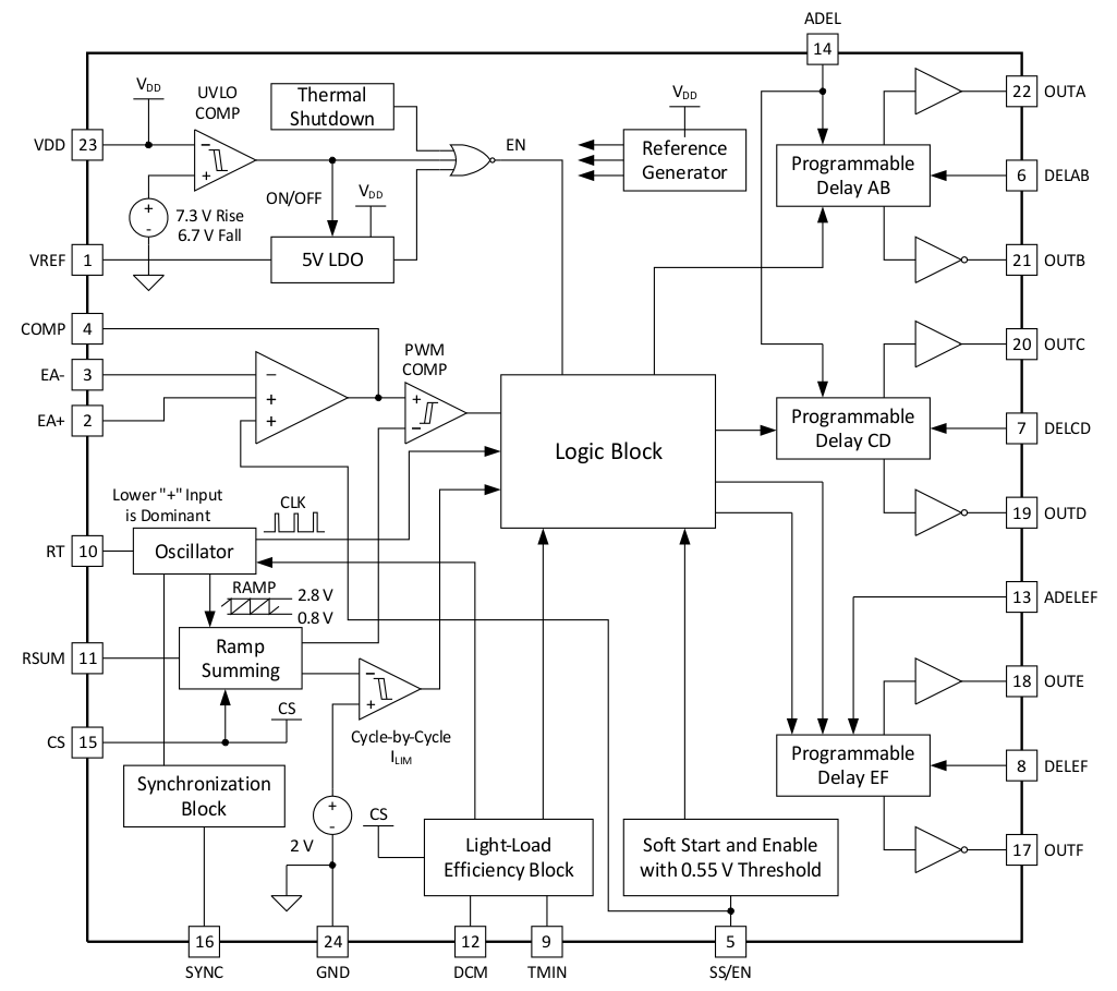
The UCC28950 device combines all the functions necessary to control a phase-shifted full bridge power stage in a 24-pin TSSOP package. The device includes two Synchronous-Rectifier (SR), gate-drive outputs as well as the outputs needed to drive all four switches in the full-bridge circuit. The dead times between the upper and lower switches in the full bridge may be set using the DELAB and DELCD inputs. Further, this dead time may be dynamically adjusted according to the load level using the ADEL pin. This allows the user to optimize the dead time for their particular power circuit and to achieve ZVS over the entire operating range. In a similar manner, the dead times between the full bridge switches and the secondary SRs may be optimized using the DELEF input. This dead time may also be dynamically adjusted according to the load, using the ADELEF input to the controller. A DCM (Discontinuous Conduction Mode) option disables the SRs at a user settable light load in order to improve power circuit efficiency. The device enters a light-load-burst mode if the feedback loop demands a conduction time less than a user settable level (TMIN).
At higher-power levels, two or more UCC28950 devices may be easily synchronized in a Master/Slave configuration. A SS/EN input may be used to set the length of the soft start process and to turn the controller on and off. The controller may be configured for Voltage mode or Current mode control. Cycle-by-cycle current limiting is provided in Voltage mode and Peak Current mode. The switching frequency may be set over a wide range making this device suited to both IGBT and MOSFET based designs.
7.3 Feature Description
7.3.1 Start-Up Protection Logic
Before the UCC28950 controller will start up, the following conditions must be met:
- VDD voltage exceeds rising UVLO threshold 7.3-V typical.
- The 5-V reference voltage is available.
- Junction temperature is below the thermal shutdown threshold of 140°C.
- The voltage on the soft-start capacitor is not below 0.55-V typical.
If all those conditions are met, an internal enable signal EN is generated that initiates the soft start process. The duty cycle during the soft start is defined by the voltage at the SS pin, and cannot be lower than the duty cycle set by TMIN, or by cycle-by-cycle current limit circuit depending on load conditions.
7.3.2 Voltage Reference (VREF)
The accurate (±1.5%) 5-V reference voltage regulator with a short circuit protection circuit supplies internal circuitry and provides up to 20-mA external output current. Place a low ESR and ESL, preferably ceramic decoupling capacitor CREF in 1-µF to 2.2-µF range from this pin to GND as close to the related pins as possible for best performance. The only condition where the reference regulator is shut down internally is during under voltage lockout.
7.3.3 Error Amplifier (EA+, EA–, COMP)
The error amplifier has two uncommitted inputs, EA+ and EA-, with a 3-MHz unity gain bandwidth, which allows flexibility in closing the feedback loop. The EA+ is a non-inverting input, the EA– is an inverting input and the COMP is the output of the error amplifier. The input voltage common mode range, where the parameters of the error amplifier are guaranteed, is from 0.5 V to 3.6 V. The output of the error amplifier is connected internally to the non-inverting input of the PWM comparator. The range of the error amplifier output of 0.25 V to 4.25 V far exceeds the PWM comparator input ramp-signal range, which is from 0.8 V to 2.8 V. The soft-start signal serves as an additional non-inverting input of the error amplifier. The lower of the two non-inverting inputs of the error amplifier is the dominant input and sets the duty cycle where the output signal of the error amplifier is compared with the internal ramp at the inputs of the PWM comparator.
7.3.4 Soft Start and Enable (SS/EN)
The soft-start pin SS/EN is a multi-function pin used for the following operations:
- Closed loop soft start with the gradual duty cycle increase from the minimum set by TMIN up to the steady state duty cycle required by the regulated output voltage.
- Setting hiccup mode conditions during cycle-by-cycle overcurrent limit.
- On/off control for the converter.
During soft start, one of the voltages at the SS/EN or EA+ pins, whichever is lower (SS/EN – 0.55 V) or EA+ voltage (see Block Diagram), sets the reference voltage for a closed feedback loop. Both SS/EN and EA+ signals are non-inverting inputs of the error amplifier with the COMP pin being its output. Thus the soft start always goes under the closed feedback loop and the voltage at COMP pin sets the duty cycle. The duty cycle defined by the COMP pin voltage can not be shorter than TMIN pulse width set by the user. However, if the shortest duty cycle is set by the cycle-by-cycle current limit circuit, then it becomes dominant over the duty cycle defined by the COMP pin voltage or by the TMIN block.
The soft-start duration is defined by an external capacitor CSS, connected between the SS/EN pin and ground, and the internal charge current that has a typical value of 25 µA. Pulling the soft-start pin externally below 0.55 V shuts down the controller. The release of the soft-start pin enables the controller to start, and if there is no current limit condition, the duty cycle applied to the output inductor gradually increases until it reaches the steady state duty cycle defined by the regulated output voltage of the converter. This happens when the voltage at the SS/EN pin reaches and then exceeds by 0.55 V, the voltage at the EA+ pin. Thus for the given soft-start time TSS, the CSS value can be defined by Equation 1 or Equation 2:


For example, in Equation 1, if the soft-start time TSS is selected to be 10 ms, and the EA+ pin is 2.5 V, then the soft-start capacitor CSS is equal to 82 nF.
NOTE
If the converter is configured in Slave Mode, place an 825-kΩ resistor from SS pin to ground.
7.3.5 Light-Load Power Saving Features
The UCC28950 offers four different light-load management techniques for improving the efficiency of a power converter over a wide load current range.
- Adaptive Delay,
- ADEL, which sets and optimizes the dead-time control for the primary switches over a wide load current range.
- ADELEF, which sets and optimizes the delay-time control between the primary side switches and the secondary side switches.
- TMIN, sets the minimum pulse width as long as the part is not in current limit mode.
- Dynamic synchronous rectifier on/off control in DCM Mode, For increased efficiency at light loads. The DCM Mode starts when the voltage at CS pin is lower than the threshold set by the user. In DCM Mode, the synchronous output drive signals OUTE and OUTF are brought down low.
- Burst Mode, for maximum efficiency at very light loads or no load. Burst Mode has an even number of PWM TMIN pulses followed by off time. Transition to the Burst Mode is defined by the TMIN duration set by the user.
7.3.6 Adaptive Delay, (Delay between OUTA and OUTB, OUTC and OUTD (DELAB, DELCD, ADEL))
The resistor RAB from the DELAB pin, DELAB to GND, along with the resistor divider RAHI from CS pin to ADEL pin and RA from ADEL pin to GND sets the delay TABSET between one of outputs OUTA or OUTB going low and the other output going high Figure 28. The total resistance of this resistor divider should be in the range between 10 kΩ and 20 kΩ
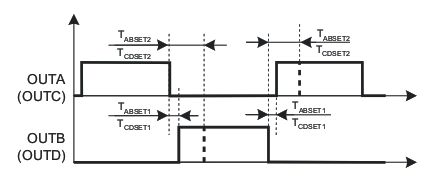 Figure 28. Delay Definitions Between OUTA and OUTB, OUTC and OUTD
This delay gradually increases as a function of the CS signal from TABSET1, which is measured at VCS = 1.8 V, to TABSET2, which is measured at the VCS = 0.2 V. This approach ensures there will be no shoot-through current during the high-side and low-side MOSFET switching and optimizes the delay for acheiving ZVS condition over a wide load current range. The ratio between the longest and shortest delays is set by the resistor divider RAHI and RA. The max ratio is achieved by tying the CS and ADEL pins together. If ADEL is connected to GND, then the delay is fixed, defined only by the resistor RAB from DELAB to GND. The delay TCDSET1 and TCDSET2 settings and their behaviour for outputs OUTC and OUTD are very similar to the one described for OUTA and OUTB. The difference is that resistor RCD connected between DELCD pin and GND sets the delay TCDSET. The ratio between the longest and shortest delays is set by the resistor divider RAHI and RA.
The delay time TABSET is defined by the following Equation 3.
The same equation is used to define the delay time TCDSET in another leg except RAB is replaced by RCD.
In these equations RAB and RCD are in kΩ and CS, the voltage at pin CS, is in volts and KA is a numerical coefficient in the range from 0 to 1. The delay time TABSET and TCDSET are in ns, and is measured at the IC pins. These equations are empirical and they are approximated from measured data. Thus, there is no unit agreement in the equations. As an example, assume RAB = 15 kΩ, CS = 1 V and KA = 0.5. Then the TABSET will be approximately 90 ns. In both Equation 3 and Equation 4, KA is the same and is defined as:

KA sets how the delay varies with the CS pin voltage as shown in Figure 29 and Figure 30.
It is recommended to start by setting KA = 0 and set TABSET and TCDSET relatively large using equations or plots in this data sheet to avoid hard switching or even shoot through current. The delay between outputs A, B and C, D set by resistors RAB and RCS accordingly. Program the optimal delays at light load first. Then by changing KA set the optimal delay for the outputs A, B at maximum current. KA for outputs C, D is the same as for A,D. Usually outputs C, D always have ZVS if sufficient delay is provided.
NOTE
The allowed resistor range on DELAB and DELCD, RAB and RCD is 13 kΩ to 90 kΩ.
RA and RAHI define the portion of voltage at pin CS applied to the pin ADEL (See Figure 48). KA defines how significantly the delay time depends on CS voltage. KA varies from 0, where ADEL pin is shorted to ground (RA = 0) and the delay does not depend on CS voltage, to 1, where ADEL is tied to CS (RAHI = 0). Setting KA, RAB and RCD provides the ability to maintain optimal ZVS conditions of primary switches over load current because the voltage at CS pin includes the load current reflected to the primary side through the current sensing circuit. The plots in Figure 29 and Figure 30 show the delay time settings as a function of CS voltage and KA for two different conditions: RAB = RCD = 13 kΩ (Figure 29) and RAB = RCD = 90 kΩ (Figure 30).
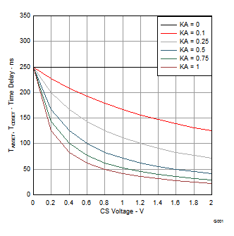 Figure 29. Delay Time Set TABSET and TCDSET
(Over CS voltage variation and selected KA for RAB and RCD equal 13 kΩ)
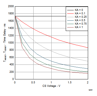 Figure 30. Delay time set TABSET and TCDSET
(Over CS voltage variation and selected KA for RAB and RCD equal 90 kΩ)
7.3.7 Adaptive Delay (Delay between OUTA and OUTF, OUTB and OUTE (DELEF, ADELEF))
The resistor REF from the DELEF pin to GND along with the resistor divider RAEFHI from CS pin to ADELEF pin and RAEF from ADELEF pin to GND sets equal delays TAFSET and TBESET between outputs OUTA or OUTB going low and related output OUTF or OUTE going low Figure 31. The total resistance of this resistor divider should be in the range between 10kΩ and 20kΩ.
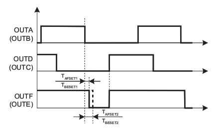 Figure 31. Delay Definitions Between OUTA and OUTF, OUTB and OUTE
These delays gradually increase as function of the CS signal from TAFSET1, which is measured at VCS = 0.2 V, to TAFSET2, which is measured at VCS = 1.8 V. This is opposite to the DELAB and DELCD behavior and this delay is longest (TAFSET2) when the signal at CS pin is maximized and shortest (TAFSET1) when the CS signal is minimized. This approach will reduce the synchronous rectifier MOSFET body diode conduction time over a wide load current range thus improving efficiency . The ratio between the longest and shortest delays is set by the resistor divider RAEFHI and RAEF. If CS and ADELEF are tied, the ratio is maximized. If ADELEF is connected to GND, then the delay is fixed, defined only by resistor REF from DELEF to GND.
The delay time TAFSET is defined by the following Equation 6. Equation 6 also defines the delay time TBESET.

In this equation REF is in kΩ, the CS, which is the voltage at pin CS, is in volts and KEF is a numerical gain factor of CS voltage from 0 to 1. The delay time TAFSET is in ns, and is measured at the IC pins. This equation is an empirical approximation of measured data, thus, there is no unit agreement in it. As an example, assume REF = 15 kΩ, CS = 1 V and KEF = 0.5. Then the TAFSET is going to be 41.7 ns. KEF is defined as:
RAEF and RAEFHI define the portion of voltage at pin CS applied to the pin ADELEF (See Figure 48). KEF defines how significantly the delay time depends on CS voltage. KEF varies from 0, where ADELEF pin is shorted to ground (RAEF = 0) and the delay does not depend on CS voltage, to 1, where ADELEF is tied to CS (RAEFHI = 0).
NOTE
The allowed resistor range on DELEF, REF is 13 kΩ to 90 kΩ.
The plots in Figure 32 and Figure 33 show delay time settings as function of CS voltage and KEF for two different conditions: REF = 13kΩ (Figure 32) and REF = 90kΩ (Figure 33)
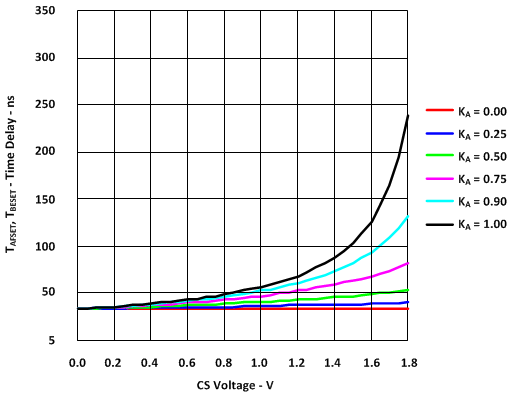 Figure 32. Delay Time TAFSET and TBESET
(Over CS Voltage and Selected KEF for REF equal 13 kΩ)
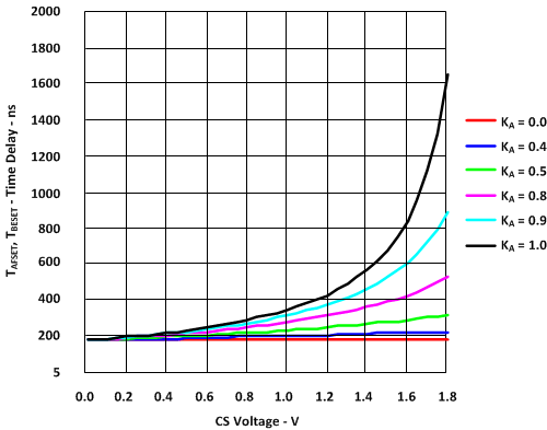 Figure 33. Delay Time TAFSET and TBESET
(Over CS Voltage and Selected KEF for REF equal 90 kΩ)
7.3.8 Minimum Pulse (TMIN)
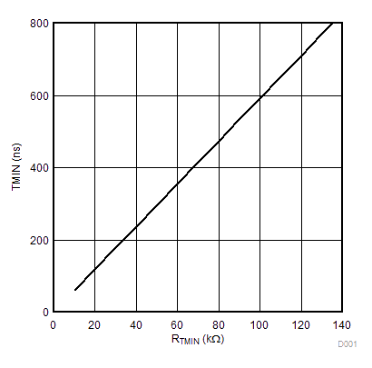
The resistor RTMIN from the TMIN pin to GND sets a fixed minimum pulse width. This pulse is applied to the transformer and enables ZVS at light load. If the output PWM pulse demanded by the feedback loop is shorter than TMIN, then the controller proceeds to burst mode operation where an even number of TMIN pulses are followed by the off time dictated by the feedback loop. The proper selection of the TMIN duration is dictated by the time it takes to raise sufficient magnetizing current in the power transformer to maintain ZVS. The TMIN pulse is measured from the rising edge of OUTA to the falling edge of OUTD – or from the rising edge of OUTB to the falling edge of OUTC. The minimum pulse TMIN is then defined by Equation 8.

Where TMIN is in ns and RTMIN is in kΩ The pulse width measured at the transformer will be modified (usually increased) by various propagation and response time delays in the power circuit. Because of the propagation and response time delays in the power circuit, selecting the correct TMIN setting will be an iterative process.
NOTE
The minimum allowed resistor on TMIN, RTMIN is 10 kΩ.
The related plot is shown in Figure 34.
The value of minimum duty cycle DMIN is determined by Equation 9.

Here, FSW(osc) is oscillator frequency in kHz, TMIN is the minimum pulse in ns and DMIN is in percent.
7.3.9 Burst Mode
If the converter is commanding a duty cycle lower than TMIN, then the controller will go into Burst Mode. The controller will always deliver an even number of Power cycles to the Power transformer. The controller always stops its bursts with an OUTB and an OUTC power delivery cycle. If the controller is still demanding a duty cycle less than TMIN, then the controller goes into shut down mode. Then it waits until the converter is demanding a duty cycle equal or higher than TMIN before the controller puts out TMIN or a PWM duty cycle as dictated by COMP voltage pin.
7.3.10 Switching Frequency Setting
Connecting an external resistor RT between the RT pin and VREF pins sets the fixed frequency operation and configures the controller as a master providing synchronization output pulses at SYNC pin with 0.5 duty cycle and frequency equal to the internal oscillator. To set the converter in slave mode, connect the external resistor RT between the RT pin to GND and place an 825-kΩ resistor from the SS pin to GND in parallel with the SS_EN capacitor. This configures the controller as a slave. The slave controller operates with 90° phase shift relative to the master converter if their SYNC pins are tied together. The switching frequency of the converter is equal to the frequency of output pulses. The following Equation 10 defines the nominal switching frequency of the converter configured as a master (resistor RT between the RT pin and VREF). On the UCC28950 there is an internal clock oscillator frequency which is twice as that of the controller's output frequency.
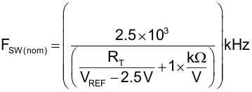
In this equation RT is in kΩ, VREF is in volts and FSW(nom) is in kHz. This is also an empirical approximation and thus, there is no unit agreement. Assume for example, VREF = 5 V, RT = 65 kΩ. Then the switching frequency FSW(nom) is going to be 92.6 kHz.
Equation 11 defines the nominal switching frequency of converter if the converter configured as a slave and the resistor RT is connected between the RT pin and GND.
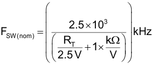
In this equation the RT is in kΩ, and FSW(nom) is in kHz. Notice that for VREF = 5 V, Equation 10 and Equation 11 yield the same results.
The plot in Figure 35 shows how FSW(nom) depends on the resistor RT value when the VREF = 5 V. As it is seen from Equation 10 and Equation 11, the switching frequency FSW(nom) is set to the same value for either master or slave configuration provided the same resistor value RT is used.
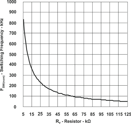 Figure 35. Converter Switching Frequency FSW(nom) Over resistor RT Value
7.3.11 Slope Compensation (RSUM)
Slope compensation is needed to prevent a sub-harmonic oscillation in a controller operating in peak current mode (PCM) control or during cycle-by-cycle current limit at duty cycles above 50% (some publications suggest it may happen at D < 50%). Slope compensation in the UCC28950 adds an additional ramp signal to the CS signal and is applied:
- To the PWM comparator in the case of peak current mode control.
- To the input of the cycle-by-cycle comparator.
At low duty cycles and light loads the slope compensation ramp reduces the noise sensitivity of Peak Current Mode control.
Placing a resistor from the RSUM pin to ground allows the controller to operate in PCM control. Connecting a resistor from RSUM to VREF switches the controller to voltage mode control (VMC) with the internal PWM ramp. In VMC the resistor at RSUM provides CS signal slope compensation for operation in cycle-by-cycle current limit. That is, in VMC, the slope compensation is applied only to the cycle-by-cycle comparator while in PCM the slope compensation is applied to both the PWM and cycle-by-cycle current limit comparators. The operation logic of the slope compensation circuit is shown in Figure 36.
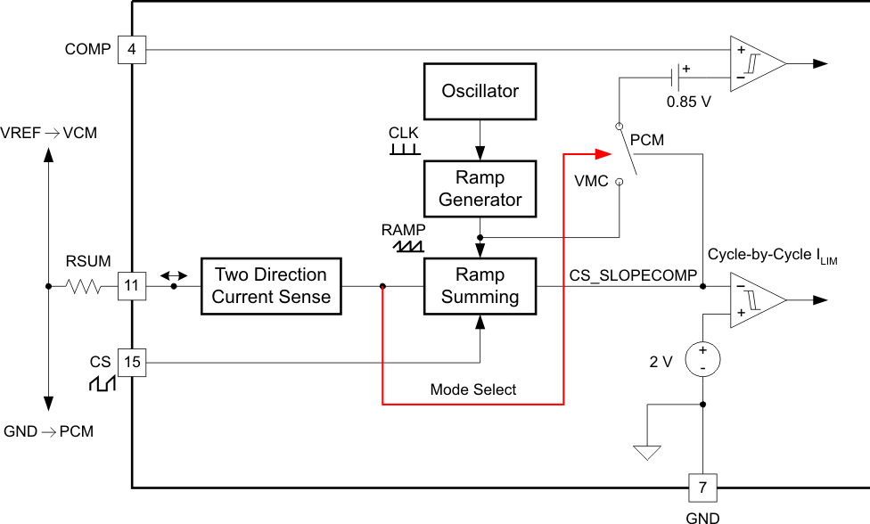 Figure 36. The Operation Logic of Slope Compensation Circuit
Too much slope compensation reduces the benefits of PCM control. In the case of cycle-by-cycle current limit, the average current limit becomes lower and this might reduce the start-up capability into large output capacitances.
The optimum compensation ramp varies, depending on duty cycle, LOUT and LMAG. A good starting point in selecting the amount of slope compensation is to set the slope compensation ramp to be half the inductor current ramp downslope (inductor current ramp during the off time). The inductor current ramp downslope – as seen at the CS pin input, and neglecting the effects of any filtering at the CS pin, will be:

Where, VOUT is the converter’s output voltage of the converter, LOUT is the output inductor value, a1 is the transformer turns ratio (Np/Ns), CTRAT is the current transformer ratio (Ip/Is, typically 100:1). Selection of LOUT, a1 and CTRAT are described elsewhere in this document. The total slope compensation is 0.5 m0. Part of this ramp will be due to magnetizing current in the transformer, the rest is added by an appropriately chosen resistor from RSUM to ground.
The slope of the additional ramp, me, added to the CS signal by placing a resistor from RSUM to ground is defined by Equation 13.

If the resistor from the RSUM pin is connected to the VREF pin, then the controller operates in voltage mode control, still having the slope compensation ramp added to the CS signal used for cycle-by-cycle current limit. In this case the slope is defined by Equation 14.

In Equation 13 and Equation 14, VREF is in volts, RSUM is in kΩ and me is in V/μs. These are empirically derived equations without units agreement. As an example, substituting VREF = 5V and RSUM = 40 kΩ, yields the result 0.125 V/μs. The related plot of me as a function of RSUM is shown in Figure 37, Because VREF = 5V, the plots generated from Equation 13 and Equation 14 coincide.
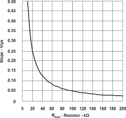 Figure 37. Slope of the Added Ramp Over Resistor RSUM
NOTE
The recommended resistor range for RSUM is 10 kΩ to 1 MΩ.
7.3.12 Dynamic SR ON/OFF Control (DCM Mode)
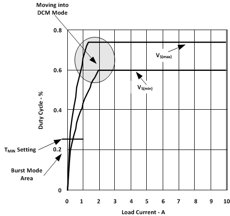
The voltage at the DCM pin provided by the resistor divider RDCMHI between VREF pin and DCM, and RDCM from DCM pin to GND, sets the percentage of 2-V current limit threshold for the Current Sense pin, (CS). If the CS pin voltage falls below the DCM pin threshold voltage, then the controller initiates the light load power saving mode, and shuts down the synchronous rectifiers, OUTE and OUTF. If the CS pin voltage is higher than the DCM pin threshold voltage, then the controller runs in CCM mode. Connecting the DCM pin to VREF makes the controller run in DCM mode and shuts both Outputs OUTE and OUTF. Shorting the DCM pin to GND disables the DCM feature and the controller runs in CCM mode under all conditions.
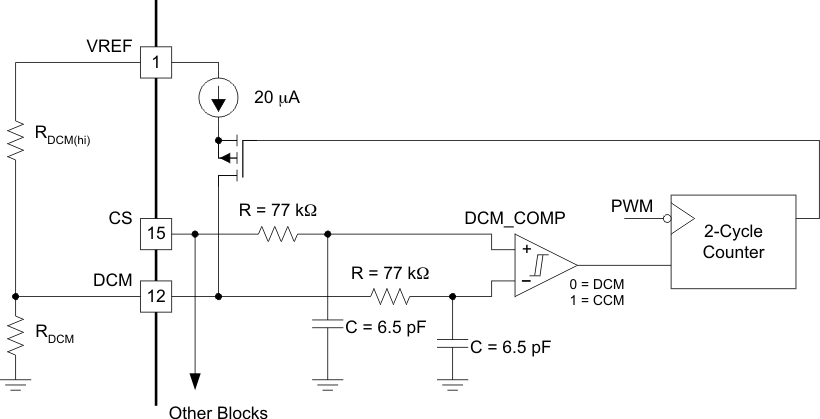 Figure 38. DCM Functional Block
A nominal 20-µA switched current source is used to create hysteresis. The current source is active only when the system is in DCM Mode. Otherwise, it is inactive and does not affect the node voltage. Therefore, when in the DCM region, the DCM threshold is the voltage divider plus ΔV explained in Equation 15. When in the CCM region, the threshold is the voltage set by the resistor divider. When the CS pin reaches the threshold set on the DCM pin, the system waits to see two consecutive falling edge PWM cycles before switching from CCM to DCM and vice-versa. The magnitude of the hysteresis is a function of the external resistor divider impedance. The hysteresis can be calculated using the following Equation 15:

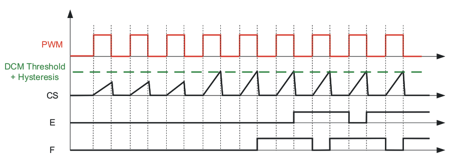 Figure 40. Moving from DCM to CCM Mode
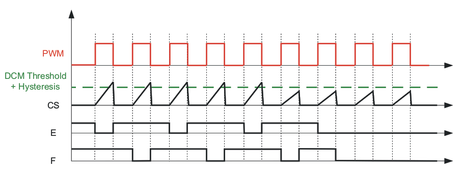 Figure 41. Moving from CCM to DCM Mode
DCM must be used in order to prevent reverse current in the output inductor which could cause the synchronous FETS to fail.
The controller must switch to DCM mode at a level where the output inductor current is positive. If the output inductor current is negative when the controller switches to DCM mode then the synchronous FETs will see a large VDS spike and may fail.
7.3.13 Current Sensing (CS)
The signal from the current sense pin is used for cycle-by-cycle current limit, peak-current mode control, light-load efficiency management and setting the delay time for outputs OUTA, OUTB, OUTC, OUTD and delay time for outputs OUTE, OUTF. Connect the current sense resistor RCS between CS and GND. Depending on layout, to prevent a potential electrical noise interference, it is recommended to put a small R-C filter between the RCS resistor and the CS pin.
7.3.14 Cycle-by-Cycle Current Limit Current Protection and Hiccup Mode
The cycle-by-cycle current limit provides peak current limiting on the primary side of the converter when the load current exceeds its predetermined threshold. For peak current mode control, a certain leading edge blanking time is needed to prevent the controller from false tripping due to switching noise. An internal 30-ns filter at the CS input is provided. The total propagation delay TCS from CS pin to outputs is 100 ns. An external RC filter is still needed if the power stage requires more blanking time. The 2.0-V ±3% cycle-by-cycle current limit threshold is optimized for efficient current transformer based sensing. The duration when a converter operates at cycle-by-cycle current limit depends on the value of soft-start capacitor and how severe the overcurrent condition is. This is achieved by the internal discharge current IDS Equation 16 and Equation 17 at SS pin.


The soft-start capacitor value also determines the so called hiccup mode off-time duration. The behavior of the converter during different modes of operation, along with related soft start capacitor charge/discharge currents are shown in Figure 42.
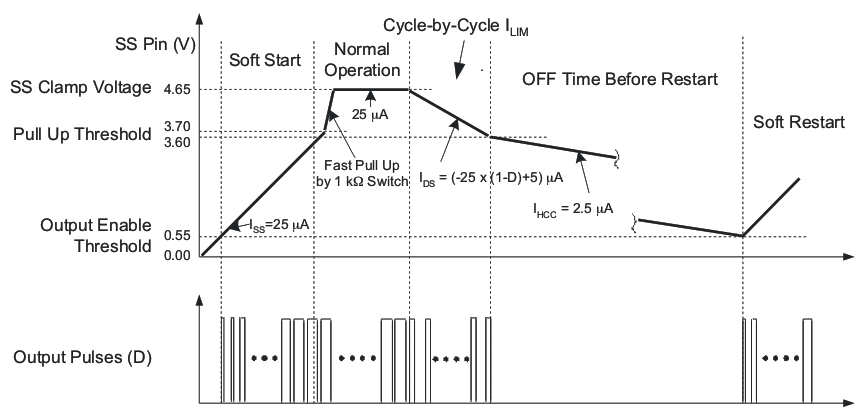 Figure 42. Timing Diagram of Soft-Start Voltage VSS
The largest discharge current of 20 µA is when the duty cycle is close to zero. This current sets the shortest operation time during the cycle-by-cycle current limit which is defined as:


Thus, if the soft-start capacitor CSS = 100 nF is selected, then the TCL(on) time will be 5 ms.
To calculate the hiccup off time TCL(off) before the restart, the following Equation 20 or Equation 21 needs to be used:


With the same soft start capacitor value 100 nF, the off time before the restart is going to be 122 ms. Notice, that if the overcurrent condition happens before the soft start capacitor voltage reaches the 3.7-V threshold during start up, the controller limits the current but the soft start capacitor continues to be charged. As soon as the 3.7-V threshold is reached, the soft-start voltage is quickly pulled up to the 4.65-V threshold by an internal 1-kΩ RDS(on) switch and the cycle-by-cycle current limit duration timing starts by discharging the soft start capacitor. Depending on specific design requirements, the user can override this default behavior by applying external charge or discharge currents to the soft start capacitor. The whole cycle-by-cycle current limit and hiccup operation is shown in Figure 42. In this example the cycle-by-cycle current limit lasts about 5 ms followed by 122 ms of off time.
Similarly to the overcurrent condition, the hiccup mode with the restart can be overridden by the user if a pullup resistor is connected between the SS and VREF pins. If the pullup current provided by the resistor exceeds 2.5 µA, then the controller remains in the latch off mode. In this case, an external soft-start capacitor value should be calculated with the additional pull-up current taken into account. The latch off mode can be reset externally if the soft-start capacitor is forcibly discharged below 0.55 V or the VDD voltage is lowered below the UVLO threshold.
7.3.15 Synchronization (SYNC)
The UCC28950 allows flexible configuration of converters operating in synchronized mode by connecting all SYNC pins together and by configuration of the controllers as master and/or slaves. The controller configured as master (resistor between RT and VREF) provides synchronization pulses at the SYNC pin with the frequency equal to 2X the converter frequency FSW(nom) and 0.5 duty cycle. The controller configured as a slave (resistor between RT and GND and 825-kΩ resistor between SS_EN pin to GND) does not generate the synchronization pulses. The Slave controller synchronizes its own clock to the falling edge of the synchronization signal thus operating 90° phase shifted versus the master converter’s frequency FSW(nom).
The output inductor in a full bridge converter sees a switching frequency which is twice that seen by the transformer. In the case of the UCC28950 this means that the output inductor operates at 2 x FSW(nom). This means that the 90° phase shift between master and slave controllers gives a 180° phase shift between the currents in the output inductors and hence maximum ripple cancellation. For more information about synchronizing more than two UCC28950 devices, see Synchronizing Three or More UCC28950 Phase-Shifted, Full-Bridge Controllers, SLUA609.
If the synchronization feature is not used then the SYNC pin may be left floating, but connecting the SYNC pin to GND via a 10-kΩ resistor will reduce noise pickup and switching frequency jitter.
- If any converter is configured as a slave, the SYNC frequency must be greater than or equal to 1.8 times the converter frequency.
- Slave converter does not start until at least one synchronization pulse has been received.
- If any or all converters are configured as slaves, then each converter operates at its own frequency without synchronization after receiving at least one synchronization pulse. Thus, If there is an interruption of synchronization pulses at the slave converter, then the controller uses its own internal clock pulses to maintain operation based on the RT value that is connected to GND in the slave converter.
- In master mode, SYNC pulses start after SS pin passes its enable threshold which is 0.55 V.
- Slave starts generating SS/EN voltage even though synchronization pulses have not been received.
- It is recommended that the SS on the master controller starts before the SS on the slave controller; therefore SS/EN pin on master converter must reach its enable threshold voltage before SS/EN on the slave converter starts for proper operation. On the same note, it’s recommended that TMIN resistors on both master and slave are set at the same value.
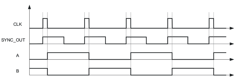 Figure 43. SYNC_OUT (Master Mode) Timing Diagram
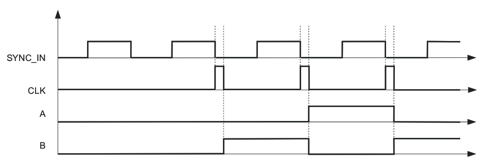 Figure 44. SYNC_IN (Slave Mode) Timing Diagram
7.3.16 Outputs (OUTA, OUTB, OUTC, OUTD, OUTE, OUTF)
- All MOSFET control outputs have 0.2-A drive capability.
- The control outputs are configured as P-MOS and N-MOS totem poles with typical RDS(on) 20 Ω and 10 Ω accordingly.
- The control outputs are capable of charging 100-pF capacitor within 12 ns and discharge within 8 ns.
- The amplitude of output control pulses is equal to VDD.
- Control outputs are designed to be used with external gate MOSFET/IGBT drivers.
- The design is optimized to prevent the latch up of outputs and verified by extensive tests.
The UCC28950 device has outputs OUTA, OUTB driving the active leg, initiating the duty cycle leg of power MOSFETs in a phase-shifted full bridge power stage, and outputs OUTC, OUTD driving the passive leg, completing the duty cycle leg, as it is shown in the typical timing diagram in Figure 46. Outputs OUTE and OUTF are optimized to drive the synchronous rectifier MOSFETs (Figure 48). These outputs have 200-mA peak-current capabilities and are designed to drive relatively small capacitive loads like inputs of external MOSFET or IGBT drivers. Recommended load capacitance should not exceed 100 pF. The amplitude of the output signal is equal to the VDD voltage.
7.3.17 Supply Voltage (VDD)
Connect this pin to a bias supply in the range from 8 V to 17 V. Place high quality, low ESR and ESL, at least 1-µF ceramic bypass capacitor CVDD from this pin to GND. It is recommended to use a 10-Ω resistor in series from the bias supply to the VDD pin to form an RC filter with the CVDD capacitor.
7.3.18 Ground (GND)
All signals are referenced to this node. It is recommended to have a separate quiet analog plane connected in one place to the power plane. The analog plane connects the components related to the pins VREF, EA+, EA-, COMP, SS/EN, DELAB, DELCD, DELEF, TMIN, RT, RSUM. The power plane connects the components related to the pins DCM, ADELEF, ADEL, CS, SYNC, OUTF, OUTE, OUTD, OUTC, OUTB, OUTA, and VDD. An example of layout and ground planes connection is shown in Figure 45.
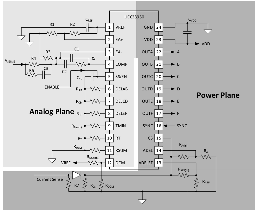 Figure 45. Layout Recommendation for Analog and Power Planes
7.4 Device Functional Modes
The UCC28950 has a number of operational modes. These modes are described in detail in Feature Description.
- Current mode(1). The UCC28950 device will operate in current mode control if the RSUM pin is connected to GND through a resistor (RSUM) . The resistor sets the amount of slope compensation.
- Voltage mode(1). The UCC28950 device will operate in voltage mode control if the RSUM pin is connected to VREF through a resistor (RSUM). The resistor value is chosen to give the correct amount of slope compensation for operation in current limit mode (cycle-by-cycle current limit).
- DCM mode. The UCC28950 device enters DCM mode if the signal at the CS pin falls below the level set by the resistor at the DCM pin. The SR drives (OUTE and OUTF) are turned off and secondary rectification is through the body diodes of the SRs.
- Burst mode. The UCC28950 device enters burst mode if the pulse width demanded by the feedback signal falls below the width set by the resistor at the TMIN pin.
- Master mode. This is the default operation mode of the UCC28950 device and is the mode used if there is only one UCC28950 device in the system. Connect the timing resistor (RT) from the RT pin to VREF. In a system with more than one UCC28950, one will be configured as the master and the others as slaves(1).
- Slave mode. The slave controller will operate with a 90° phase shift relative to the Master (providing their SYNC pins are tied together). Connect the timing resistor (RT) from the RT pin to GND and connect an 825 kΩ resistor from the SS/EN pin to GND(1).
- Synchronized mode. If a UC28950 is configured as a slave then its SYNC pin is used as an input. The slave will synchronize its internal oscillator at 90° to the signal at its SYNC pin. App note slua609 discusses how multiple Slave controllers may be synchronized to a single master oscillator.
- Hiccup mode. This mode provides overload protection to the power circuit. The UCC28950 device stops switching after a certain time in current limit. It starts again (soft start) after a delay time. The user can control the time spent in current limit before switching is stopped and the delay time before the soft start happens.
- Current-limit mode. The UCC28950 device will provide cycle-by-cycle current limiting if the signal at the CS pin reaches 2V.
- Latch-off mode. Connect a resistor between the SS pin and VREF. The UCC28950 will then latch off if the controller enters Current Limit mode. (1)
