SLUSDB2A August 2018 – December 2021 UCC28951
PRODUCTION DATA
- 1 Features
- 2 Applications
- 3 Description
- 4 Revision History
- 5 Pin Configuration and Functions
- 6 Specifications
-
7 Detailed Description
- 7.1 Overview
- 7.2 Functional Block Diagram
- 7.3
Feature Description
- 7.3.1 Start-Up Protection Logic
- 7.3.2 Voltage Reference (VREF)
- 7.3.3 Error Amplifier (EA+, EA–, COMP)
- 7.3.4 Soft-Start and Enable (SS/EN)
- 7.3.5 Light-Load Power Saving Features
- 7.3.6 Adaptive Delay, (Delay Between OUTA and OUTB, OUTC and OUTD (DELAB, DELCD, ADEL))
- 7.3.7 Adaptive Delay (Delay Between OUTA and OUTF, OUTB and OUTE (DELEF, ADELEF)
- 7.3.8 Minimum Pulse (TMIN)
- 7.3.9 Burst Mode
- 7.3.10 Switching Frequency Setting
- 7.3.11 Slope Compensation (RSUM)
- 7.3.12 Dynamic SR ON/OFF Control (DCM Mode)
- 7.3.13 Current Sensing (CS)
- 7.3.14 Cycle-by-Cycle Current Limit Current Protection and Hiccup Mode
- 7.3.15 Synchronization (SYNC)
- 7.3.16 Outputs (OUTA, OUTB, OUTC, OUTD, OUTE, OUTF)
- 7.3.17 Supply Voltage (VDD)
- 7.3.18 Ground (GND)
- 7.4 Device Functional Modes
-
8 Application and Implementation
- 8.1 Application Information
- 8.2
Typical Application
- 8.2.1 Design Requirements
- 8.2.2
Detailed Design Procedure
- 8.2.2.1 Power Loss Budget
- 8.2.2.2 Preliminary Transformer Calculations (T1)
- 8.2.2.3 QA, QB, QC, QD FET Selection
- 8.2.2.4 Selecting LS
- 8.2.2.5 Selecting Diodes DB and DC
- 8.2.2.6 Output Inductor Selection (LOUT)
- 8.2.2.7 Output Capacitance (COUT)
- 8.2.2.8 Select FETs QE and QF
- 8.2.2.9 Input Capacitance (CIN)
- 8.2.2.10 Current Sense Network (CT, RCS, R7, DA)
- 8.2.3 Application Curves
- 9 Power Supply Recommendations
- 10Layout
- 11Device and Documentation Support
Package Options
Mechanical Data (Package|Pins)
- PW|24
Thermal pad, mechanical data (Package|Pins)
Orderable Information
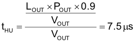
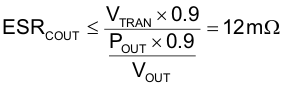
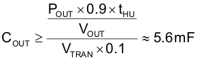
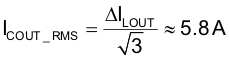
8.2.2.7 Output Capacitance (COUT)
The output capacitor is selected based on holdup and transient (VTRAN) load requirements.
The time it takes LOUT to change 90% of its full load current is calculated in Equation 67:
During load transients most of the current will immediately go through the capacitors equivalent series resistance (ESRCOUT). Equation 68 and Equation 69 are used to select ESRCOUT and COUT based on a 90% load step in current. The ESR is selected for 90% of the allowable transient voltage (VTRAN), while the output capacitance (COUT) is selected for 10% of VTRAN.
Before selecting the output capacitor, the output capacitor RMS current (ICOUT_RMS) must be calculated using Equation 70.
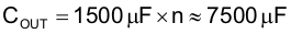
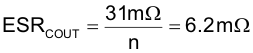
To meet the design requirements five 1500-µF, aluminum electrolytic capacitors are chosen for the design from United Chemi-Con™, part number EKY-160ELL152MJ30S. These capacitors have an ESR of 31 mΩ.
The number of output capacitors (n) is 5.
The total output capacitance is calculated usingEquation 71:
The effective output capacitance ESR is calculated usingEquation 72:
Calculate output capacitor loss (PCOUT) using Equation 73:

Recalculate the remaining Power Budget using Equation 74:
