SLUSDB2A August 2018 – December 2021 UCC28951
PRODUCTION DATA
- 1 Features
- 2 Applications
- 3 Description
- 4 Revision History
- 5 Pin Configuration and Functions
- 6 Specifications
-
7 Detailed Description
- 7.1 Overview
- 7.2 Functional Block Diagram
- 7.3
Feature Description
- 7.3.1 Start-Up Protection Logic
- 7.3.2 Voltage Reference (VREF)
- 7.3.3 Error Amplifier (EA+, EA–, COMP)
- 7.3.4 Soft-Start and Enable (SS/EN)
- 7.3.5 Light-Load Power Saving Features
- 7.3.6 Adaptive Delay, (Delay Between OUTA and OUTB, OUTC and OUTD (DELAB, DELCD, ADEL))
- 7.3.7 Adaptive Delay (Delay Between OUTA and OUTF, OUTB and OUTE (DELEF, ADELEF)
- 7.3.8 Minimum Pulse (TMIN)
- 7.3.9 Burst Mode
- 7.3.10 Switching Frequency Setting
- 7.3.11 Slope Compensation (RSUM)
- 7.3.12 Dynamic SR ON/OFF Control (DCM Mode)
- 7.3.13 Current Sensing (CS)
- 7.3.14 Cycle-by-Cycle Current Limit Current Protection and Hiccup Mode
- 7.3.15 Synchronization (SYNC)
- 7.3.16 Outputs (OUTA, OUTB, OUTC, OUTD, OUTE, OUTF)
- 7.3.17 Supply Voltage (VDD)
- 7.3.18 Ground (GND)
- 7.4 Device Functional Modes
-
8 Application and Implementation
- 8.1 Application Information
- 8.2
Typical Application
- 8.2.1 Design Requirements
- 8.2.2
Detailed Design Procedure
- 8.2.2.1 Power Loss Budget
- 8.2.2.2 Preliminary Transformer Calculations (T1)
- 8.2.2.3 QA, QB, QC, QD FET Selection
- 8.2.2.4 Selecting LS
- 8.2.2.5 Selecting Diodes DB and DC
- 8.2.2.6 Output Inductor Selection (LOUT)
- 8.2.2.7 Output Capacitance (COUT)
- 8.2.2.8 Select FETs QE and QF
- 8.2.2.9 Input Capacitance (CIN)
- 8.2.2.10 Current Sense Network (CT, RCS, R7, DA)
- 8.2.3 Application Curves
- 9 Power Supply Recommendations
- 10Layout
- 11Device and Documentation Support
Package Options
Mechanical Data (Package|Pins)
- PW|24
Thermal pad, mechanical data (Package|Pins)
Orderable Information
8.2.2.10.1 Voltage Loop Compensation Recommendation
For best results in the voltage loop, TI recommends using a Type 2 or Type 3 compensation network (Figure 8-6). A Type 2 compensation network does not require passive components CZ2 and RZ2. Type 1 compensation is not versatile enough for a phase-shifted full bridge. When evaluating the COMP pin for best results, TI recommends placing a 1-kΩ resistor between the scope probe and the COMP pin of the UCC28951.
 Figure 8-6 Type 3
Compensation Evaluation
Figure 8-6 Type 3
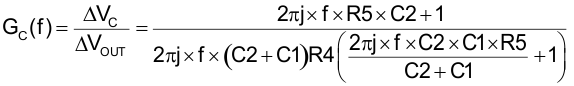
Compensation EvaluationCompensating the feedback loop can be accomplished by properly selecting the feedback components (R5, C1 and C2). These components are placed as close as possible to pin 3 and 4 of the controller. A Type 2 compensation network is designed in this example.
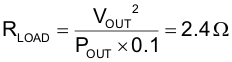
Calculate load impedance at 10% load (RLOAD) :
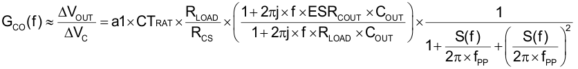
Approximate control to output transfer function (GCO(f)) as a function of frequency:
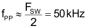
Calculate double pole frequency of GCO(f):
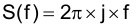
Calculate angular velocity:
Compensate the voltage loop with Type 2 feedback network. The following transfer function is the compensation gain as a function of frequency (GC(f)):
Calculate voltage loop feedback resistor (R5) based on the crossing the voltage loop (fC) over at a 10th of the double pole frequency (fPP):
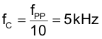
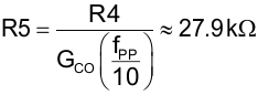
The standard resistor selcted for R5 is 27.4 kΩ.
Calculate the feedback capacitor (C2) to give added phase at crossover:
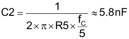
The standard capacitance value (C2) selected for the design is 5.6 nF.
Put a pole at two times fC:
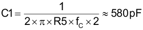
The standard capacitance value (C1) selected for the design is 560 pF.
Use Equation 126 to calculate the loop gain as a function of frequency (TV(f)) in dB.
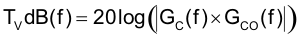
Plot a theoretical loop gain and phase to graphically confirm loop stability. The theoretical loop gain crosses over at roughly 3.7 kHz with a phase margin of greater than 90 degrees.
 Figure 8-7 Loop Gain
and Phase vs Frequency
Figure 8-7 Loop Gain
and Phase vs FrequencyTI recommends confirming the loop stability of the final design with transient testing and/or a network analyzer. Adjust the compensation (GC(f)) feedback as necessary.
where
- loop gain (TVdB(f))
- loop phase (ΦTV(f))
To limit overshoot during the power up sequence, the UCC28951 has a soft-start function (SS, Pin 5). In this application the soft-start time is 15 ms (tSS).

The standard capacitor (CSS) selected for this design is 150 nF.
This application presents a fixed delay approach to achieving ZVS from 100% load down to 50% load. Adaptive delays can be generated by connecting the ADEL and ADELEF pins to the CS pin as shown in Figure 8-8 .
 Figure 8-8 Adaptive
Delays
Figure 8-8 Adaptive
DelaysWhen the converter is operating below 50% load, the converter operates in valley switching. To achieve zero voltage switching on switch node of QBd, the turn-on (tABSET) delays of FETs QA and QB must be initially set based on the interaction of LS and the theoretical switch node capacitance. The following equations are used to set tABSET initially.
Equate shim inductance to two times COSS capacitance using Equation 129:
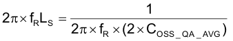
Calculate tank frequency using Equation 130:

Set initial tABSET delay time and adjust as necessary.
The 2.25 factor of the tABSET equation was derived from empirical test data and may vary based on individual design differences.
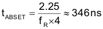
The resistor divider formed by RA and RAHI programs the tABSET, tCDSET delay range of the controller. The standard resistor value RAHI selected is 8.25 kΩ.
tABSET can be programmed between 30 ns to 1000 ns.
The voltage at the ADEL input of the controller (VADEL) must be set with RA based on the following conditions:
- If tABSET > 155 ns, set VADEL = 0.2 V. tABSET can be programmed between 155 ns and 1000 ns.
- If tABSET ≤ 155 ns, set VADEL = 1.8 V. tABSET can be programmed between 29 ns and 155 ns.
Based on VADEL selection, calculate RA:
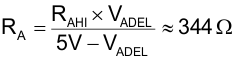
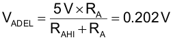
The closest standard resistor value for RA selected is 348 Ω.
Recalculate VADEL based on resistor divider selection:
Resistor RAB programs tABSET. Variable CS is the voltage at the CS pin with respect to ground and ratio KA was calculated in Equation 5:
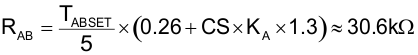
The standard resistor value for RAB selected for the design is 30.1 kΩ.
After a prototype oprational, fine tune tABSET during light-load operation to the peak and valley of the resonance between LS and the switch node capacitance. In this design, the delay was set at 10% load.
 Figure 8-9 tABSET to Achieve Valley Switching at Light Loads
Initially, set the QC and QD turn-on delays (tCDSET) for the same delay as the QA and QB turn-on delays (Pin 6). The following equations program the QC and QD turn-on delays (tCDSET) by properly selecting resistor RDELCD (Pin 7).

Resistor RCD programs tCDSET:
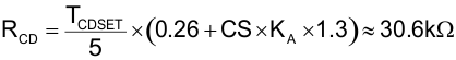
The standard resistor RCD selected for this design is 30.1 kΩ.
After a prototype operational, fine tune tCDSET during light-load operation. In this design, the CD node was set to valley switch at roughly 10% load.. Obtaining ZVS at lighter loads with switch node QDd is easier due to the reflected output current present in the primary of the transformer at FET QD and QC during the turnoff or turnon period. This behavior is due to more peak current available to energize LS before this transition, compared to the QA and QB turnoff and turnon period.
 Figure 8-10 tCDSET to Achieve Valley Switching at Light Loads
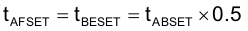
There is a programmable delay for the turnoff of FET QF after FET QA turnoff (tAFSET) and the turnoff of FET QE after FET QB turnoff (tBESET). Set these delays to 50% of tABSET to ensure that the appropriate synchronous rectifier turns off before the AB ZVS transition. If this delay is too large, it causes OUTE and OUTF not to overlap correctly and creates excess body diode conduction on FETs QE and QF.
The resistor divider formed by RAEF and RAEFHI programs the tAFSET and tBESET delay range of the controller. The standard resistor value selected for RAEFHI is 8.25 kΩ.
tAFSET and tBESET can be programmed between 32 ns to 1100 ns.
The voltage at the ADELEF pin of the controller (VADELEF) needs to be set with RAEF based on the following conditions.
- If tAFSET < 170 ns set VADEL = 0.2 V, tABSET can be programmed between 32 ns and 170 ns.
- If tABSET > or = 170 ns set VADEL = 1.7 V, tABSET can be programmed between 170 ns and 1100 ns.
Based on VADELEF selection, calculate RAEF:
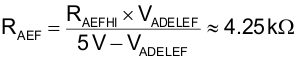
The closest standard resistor value for RAEF is 4.22 kΩ.
Recalculate VADELEF based on resistor divider selection:

The following equation was used to program tAFSET and tBESET by properly selecting resistor REF.

The standard resistor value selected for REF is 14 kΩ.
Resistor RTMIN programs the minimum on time (tMIN) that the UCC28951 (Pin 9) can demand before entering burst mode. If the UCC28951 controller tries to demand a duty cycle on time of less than tMIN the power supply goes into burst mode operation. For this design set the minimum on-time (tMIN) to 75 ns.
Set the minimum on-time by selecting RTMIN :
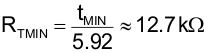
The standard resistor value for RTMIN is 13 kΩ.
A resistor from the RT pin to ground sets the converter switching frequency calculated in Equation 142.
The standard resistor value selected for RT is 61.9 kΩ.
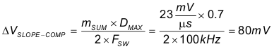
The UCC28951 provides slope compensation. The amount of slope compensation is set by the resistor RSUM. As suggested earlier, set the slope compensation ramp to be half the inductor current ramp downslope (inductor current ramp during the off time), reflected through the main transformer and current sensing networks as explained earlier in Section 7.3.11.
Calculate required slope compensation ramp:
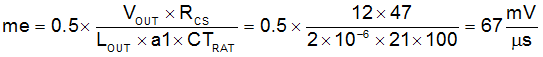
The magnetizing current of the power transformer provides part of the slope compensation ramp. The slope of this current is calculated using Equation 144 where VINHU is the minimum voltage for VOUT holdup purposes. It is the voltage at which the converter is operating at the maximum dudy cycle (DMAX) while maintaining VOUT:
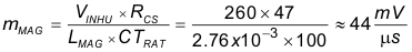
Calculate the required compensating ramp:
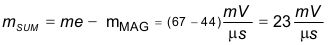
The value for the resistor, RSUM, may be found from the graph in Figure 7-10, calculated from rearranged versions of Equation 13, or calculated by Equation 13, depending on whether the controller is operating in current mode or voltage control mode. This design uses current mode control and Equation 146 is rearranged and evaluated:
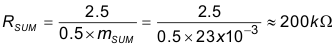
Confirm that the 300 mV allowed for the slope compensation ramp is sufficient when choosing RCS in Equation 100.
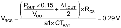
To increase efficiency at lighter loads the UCC28951 is programmed (Pin 12, DCM) under light-load conditions to disable the synchronous FETs on the secondary side of the converter (QE and QF). This threshold is programmed with resistor divider formed by RDCMHI and RDCM. This DCM threshold needs to be set at a level before the inductor current goes discontinuous. Equation 148 sets the level at which the synchronous rectifiers are disabled at roughly 15% load current.
The standard resistor value selected for RDCM is 1 kΩ.
Calculate resistor value RDCMHI.
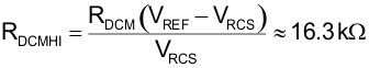
The standard resistor value for RDCMHI is 16.9 kΩ.