SLUSDB2A August 2018 – December 2021 UCC28951
PRODUCTION DATA
- 1 Features
- 2 Applications
- 3 Description
- 4 Revision History
- 5 Pin Configuration and Functions
- 6 Specifications
-
7 Detailed Description
- 7.1 Overview
- 7.2 Functional Block Diagram
- 7.3
Feature Description
- 7.3.1 Start-Up Protection Logic
- 7.3.2 Voltage Reference (VREF)
- 7.3.3 Error Amplifier (EA+, EA–, COMP)
- 7.3.4 Soft-Start and Enable (SS/EN)
- 7.3.5 Light-Load Power Saving Features
- 7.3.6 Adaptive Delay, (Delay Between OUTA and OUTB, OUTC and OUTD (DELAB, DELCD, ADEL))
- 7.3.7 Adaptive Delay (Delay Between OUTA and OUTF, OUTB and OUTE (DELEF, ADELEF)
- 7.3.8 Minimum Pulse (TMIN)
- 7.3.9 Burst Mode
- 7.3.10 Switching Frequency Setting
- 7.3.11 Slope Compensation (RSUM)
- 7.3.12 Dynamic SR ON/OFF Control (DCM Mode)
- 7.3.13 Current Sensing (CS)
- 7.3.14 Cycle-by-Cycle Current Limit Current Protection and Hiccup Mode
- 7.3.15 Synchronization (SYNC)
- 7.3.16 Outputs (OUTA, OUTB, OUTC, OUTD, OUTE, OUTF)
- 7.3.17 Supply Voltage (VDD)
- 7.3.18 Ground (GND)
- 7.4 Device Functional Modes
-
8 Application and Implementation
- 8.1 Application Information
- 8.2
Typical Application
- 8.2.1 Design Requirements
- 8.2.2
Detailed Design Procedure
- 8.2.2.1 Power Loss Budget
- 8.2.2.2 Preliminary Transformer Calculations (T1)
- 8.2.2.3 QA, QB, QC, QD FET Selection
- 8.2.2.4 Selecting LS
- 8.2.2.5 Selecting Diodes DB and DC
- 8.2.2.6 Output Inductor Selection (LOUT)
- 8.2.2.7 Output Capacitance (COUT)
- 8.2.2.8 Select FETs QE and QF
- 8.2.2.9 Input Capacitance (CIN)
- 8.2.2.10 Current Sense Network (CT, RCS, R7, DA)
- 8.2.3 Application Curves
- 9 Power Supply Recommendations
- 10Layout
- 11Device and Documentation Support
Package Options
Mechanical Data (Package|Pins)
- PW|24
Thermal pad, mechanical data (Package|Pins)
Orderable Information
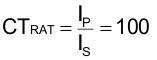
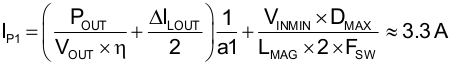
8.2.2.10 Current Sense Network (CT, RCS, R7, DA)
The CT chosen for this design has a turns ratio (CTRAT) of 100:1 in Equation 97:
Calculate nominal peak current (IP1) at VINMIN:
The peak primary current is calculated using Equation 98:
The CS pin voltage where peak current limit will trip is:

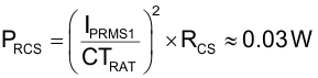
Calculate current sense resistor (RCS) and leave 300 mV for slope compensation using Equation 100. Include a 1.1 factor for margin:
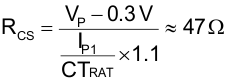
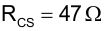
Select a standard resistor for RCS:
Estimate the power loss for RCS using Equation 102:
Calculate maximum reverse voltage (VDA) on DA using Equation 103:
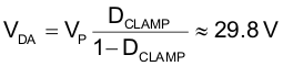
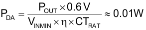
Estimate the DA power loss (PDA) using Equation 104:
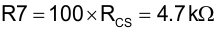
Calculate reset resistor R7:
Resistor R7 is used to reset the current sense transformer CT:
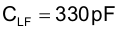
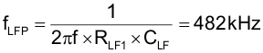
Resistor RLF1 and capacitor CLF form a low-pass filter for the current sense signal (Pin 15). For this design, chose the following values. This filter has a low frequency pole (fLFP) at 482 kHz, (which is appropriate for most applications) but may be adjusted to suit individual layouts and EMI present in the design.

The UCC28951 VREF output (Pin 1) needs a high frequency bypass capacitor to filter out high frequency noise. This pin needs at least 1 µF of high-frequency bypass capacitance (CREF).

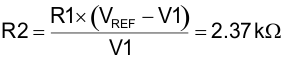
The voltage amplifier reference voltage (Pin 2, EA +) can be set with a voltage divider (R1, R2), for this design example, the error amplifier reference voltage (V1) will be set to 2.5 V. Select a standard resistor value for R1 and then calculate resistor value R2.
UCC28951 reference voltage:

Set voltage amplifier reference voltage:


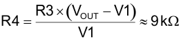
The voltage divider formed by resistor R3 and R4 are chosen to set the DC output voltage (VOUT) at Pin 3 (EA-).
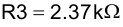
Select a standard resistor for R3:
Calculate R4 using Equation 115:
Then choose a standard resistor for R4 using Equation 116:

TI recommends using an RCD clamp to protect the output synchronous FETs from overvoltage due to switch node ringing.
 Figure 8-5 Daughter
Board Schematic
Figure 8-5 Daughter
Board Schematic