SLUSDB2A August 2018 – December 2021 UCC28951
PRODUCTION DATA
- 1 Features
- 2 Applications
- 3 Description
- 4 Revision History
- 5 Pin Configuration and Functions
- 6 Specifications
-
7 Detailed Description
- 7.1 Overview
- 7.2 Functional Block Diagram
- 7.3
Feature Description
- 7.3.1 Start-Up Protection Logic
- 7.3.2 Voltage Reference (VREF)
- 7.3.3 Error Amplifier (EA+, EA–, COMP)
- 7.3.4 Soft-Start and Enable (SS/EN)
- 7.3.5 Light-Load Power Saving Features
- 7.3.6 Adaptive Delay, (Delay Between OUTA and OUTB, OUTC and OUTD (DELAB, DELCD, ADEL))
- 7.3.7 Adaptive Delay (Delay Between OUTA and OUTF, OUTB and OUTE (DELEF, ADELEF)
- 7.3.8 Minimum Pulse (TMIN)
- 7.3.9 Burst Mode
- 7.3.10 Switching Frequency Setting
- 7.3.11 Slope Compensation (RSUM)
- 7.3.12 Dynamic SR ON/OFF Control (DCM Mode)
- 7.3.13 Current Sensing (CS)
- 7.3.14 Cycle-by-Cycle Current Limit Current Protection and Hiccup Mode
- 7.3.15 Synchronization (SYNC)
- 7.3.16 Outputs (OUTA, OUTB, OUTC, OUTD, OUTE, OUTF)
- 7.3.17 Supply Voltage (VDD)
- 7.3.18 Ground (GND)
- 7.4 Device Functional Modes
-
8 Application and Implementation
- 8.1 Application Information
- 8.2
Typical Application
- 8.2.1 Design Requirements
- 8.2.2
Detailed Design Procedure
- 8.2.2.1 Power Loss Budget
- 8.2.2.2 Preliminary Transformer Calculations (T1)
- 8.2.2.3 QA, QB, QC, QD FET Selection
- 8.2.2.4 Selecting LS
- 8.2.2.5 Selecting Diodes DB and DC
- 8.2.2.6 Output Inductor Selection (LOUT)
- 8.2.2.7 Output Capacitance (COUT)
- 8.2.2.8 Select FETs QE and QF
- 8.2.2.9 Input Capacitance (CIN)
- 8.2.2.10 Current Sense Network (CT, RCS, R7, DA)
- 8.2.3 Application Curves
- 9 Power Supply Recommendations
- 10Layout
- 11Device and Documentation Support
Package Options
Mechanical Data (Package|Pins)
- PW|24
Thermal pad, mechanical data (Package|Pins)
Orderable Information
8.1 Application Information
The high efficiency of a phase-shifted full-bridge DC-DC converter using the UCC28951 is achieved by using synchronous rectification, a control algorithm providing ZVS condition over the entire load current range, accurate adaptive timing of the control signals between primary and secondary FETs and special operating modes at light load. A simplified electrical diagram of this converter is shown in Figure 8-3. The UCC28951controller is located on the secondary side of converter, although it could be placed on the primary side as well. The secondary side lication allows easy power system level communication and better handling of some transient conditions that require fast direct control of the synchronous rectifier MOSFETs. The power stage includes primary side MOSFETs, QA, QB, QC, QD and secondary side synchronous rectifier MOSFETs, QE and QF. For example, for the 12-V output converters in server power supplies use of the center-tapped rectifier scheme with L-C output filter is a popular choice.
To maintain high efficiency at different output power conditions, the converter operates in synchronous rectification mode at mid and high output power levels, transitioning to diode rectifier mode at light load and then into burst mode as the output power becomes even lower. All of these transitions are based on current sensing on the primary side using a current sense transformer in this specific case.
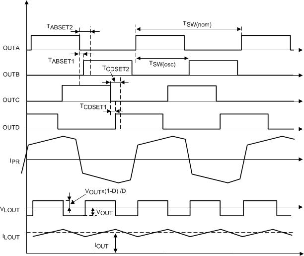
The major waveforms of the phase-shifted converter during normal operation are shown in Figure 8-1. The upper six waveforms in Figure 8-1 show the output drive signals of the controller. In normal mode, the outputs OUTE and OUTF overlap during the part of the switching cycle when both rectifier MOSFETs are conducting and the windings of the power transformer are shorted. Current, IPR, is the current flowing through the primary winding of the power transformer. The bottom four waveforms show the drain-source voltages of rectifier MOSFETs, VDS_QE and VDS_QF, the voltage at the output inductor, V LOUT, and the current through the output inductor, I LOUT. Proper timing between the primary switches and synchronous rectifier MOSFETs is critical to achieve highest efficiency and reliable operation in this mode. The controller adjusts the turn OFF timing of the rectifier MOSFETs as a function of load current to ensure minimum conduction time and reverse recovery losses of their internal body diodes.
ZVS is an important feature of relatively high input voltage converters in reducing switching losses associated with the internal parasitic capacitances of power switches and transformers. The controller ensures ZVS conditions over the entire load current range by adjusting the delay time between the primary MOSFETs switching in the same leg in accordance to the load variation. The controller also limits the minimum ON-time pulse applied to the power transformer at light load, allowing the storage of sufficient energy in the inductive components of the power stage for the ZVS transition.
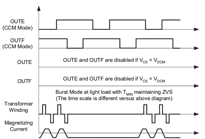
As the load current reduces from full load down to the no-load condition, the controller selects the most efficient power saving mode by moving from the normal operation mode to the discontinuous-current diode-rectification mode and, eventually, at very light-load and at no-load condition, to the burst mode. These modes and related output signals, OUTE, OUTF, driving the rectifier MOSFETs, are shown in Figure 8-2.
 Figure 8-1 Phase-Shifted Converter Waveforms
 Figure 8-2 Major
Waveforms During Transitions Between Different Operating Modes
Figure 8-2 Major
Waveforms During Transitions Between Different Operating ModesIt is necessary to prevent the reverse current flow through the synchronous rectifier MOSFETs and output inductor at light load, during parallel operation and at some transient conditions. Such reverse current results in circulating of some extra energy between the input voltage source and the load and, therefore, causes increased losses and reduced efficiency. Another negative effect of such reverse current is the loss of ZVS condition. The suggested control algorithm prevents reverse current flow, still maintaining most of the benefits of synchronous rectification by switching off the drive signals of rectifier MOSFETs in a predetermined way. At some pre-determined load current threshold, the controller disables outputs OUTE and OUTF by bringing them down to zero.
Synchronous rectification using MOSFETs requires some electrical energy to drive the MOSFETs. There is a condition below some light-load threshold when the MOSFET drive related losses exceed the saving provided by the synchronous rectification. At such light load, it is best to disable the drive circuit and use the internal body diodes of rectifier MOSFETs, or external diodes in parallel with the MOSFETs, for more efficient rectification. In most practical cases, the drive circuit needs to be disabled close to DCM mode. This mode of operation is called discontinuous-current diode-rectification mode.
At very light-load and no-load conditions, the duty cycle, demanded by the closed-feedback-loop control circuit for output voltage regulation, can be very low. This level leads to the loss of ZVS condition and increased switching losses. To avoid the loss of ZVS, the control circuit limits the minimum ON-time pulse applied to the power transformer using resistor from TMIN pin to GND. Therefore, the only way to maintain regulation at very light load and at no-load condition is to skip some pulses. The controller skips pulses in a controllable manner to avoid saturation of the power transformer. Such operation is called burst mode. In Burst Mode there are always an even number of pulses applied to the power transformer before the skipping off time. Thus, the flux in the core of the power transformer always starts from the same point during the start of every burst of pulses.