SLUSA12G December 2009 – November 2022 UCC28C40-Q1 , UCC28C41-Q1 , UCC28C42-Q1 , UCC28C43-Q1 , UCC28C44-Q1 , UCC28C45-Q1
PRODUCTION DATA
- 1 Features
- 2 Applications
- 3 Description
- 4 Revision History
- 5 Device Comparison Table
- 6 Pin Configuration and Functions
- 7 Specifications
-
8 Detailed Description
- 8.1 Overview
- 8.2 Functional Block Diagram
- 8.3 Feature Description
- 8.4 Device Functional Modes
-
9 Application and Implementation
- 9.1 Application Information
- 9.2
Typical Application
- 9.2.1 Design Requirements
- 9.2.2
Detailed Design Procedure
- 9.2.2.1 Custom Design With WEBENCH® Tools
- 9.2.2.2 Input Bulk Capacitor and Minimum Bulk Voltage
- 9.2.2.3 Transformer Turns Ratio and Maximum Duty CycleG
- 9.2.2.4 Transformer Inductance and Peak Currents
- 9.2.2.5 Output Capacitor
- 9.2.2.6 Current Sensing Network
- 9.2.2.7 Gate Drive Resistor
- 9.2.2.8 VREF Capacitor
- 9.2.2.9 RT/CT
- 9.2.2.10 Start-Up Circuit
- 9.2.2.11 Voltage Feedback Compensation
- 9.2.3 Application Curves
- 9.2.4 Power Supply Recommendations
- 9.2.5 Layout
- 10Device and Documentation Support
- 11Mechanical, Packaging, and Orderable Information
Package Options
Mechanical Data (Package|Pins)
- D|8
Thermal pad, mechanical data (Package|Pins)
Orderable Information
9.2.2.3 Transformer Turns Ratio and Maximum Duty CycleG
The transformer design starts with selecting a suitable switching frequency for the given application. The UCC28C42 is capable of switching up to 1 MHz but considerations such as overall converter size, switching losses, core loss, system compatibility, and interference with communication frequency bands generally determine an optimum frequency that should be used. For this off-line converter, the switching frequency (fSW) is selected to be 110 kHz as a compromise to minimize the transformer size and the EMI filter size, and still have acceptable losses.
The transformer primary to secondary turns ratio (NPS) can be selected based on the desired MOSFET voltage rating and the secondary diode voltage rating. Because the maximum input voltage is 265 VRMS, the peak bulk input voltage can be calculated as shown in Equation 4.

To minimize the cost of the system, a readily available 650V MOSFET is selected. Derating the maximum voltage stress on the drain to 80% of its rated value and allowing for a leakage inductance voltage spike of up to 30% of the maximum bulk input voltage, the reflected output voltage must be less than 130 V as shown in Equation 5.

The maximum primary to secondary transformer turns ratio (NPS) for a 12 V output can be selected as

A turns ratio of NPS = 10 is used in the design example.
The auxiliary winding is used to supply bias voltage to the UCC28C42-Q1. Maintaining the bias voltage above the VDD minimum operating voltage after turnon is required for stable operation. The minimum VDD operating voltage for the UCC28C42-Q1 version of the controller is 10 V. The auxiliary winding is selected to support a 12 V bias voltage so that it is above the minimum operating level but still keeps the losses low in the IC. The primary to auxiliary turns ratio (NPA) can be calculated from Equation 7:

The output diode experiences a voltage stress that is equal to the output voltage plus the reflected input voltage:

TI recommends a Schottky diode with a rated blocking voltage greater than 60 V to allow for voltage spikes due to ringing. The forward voltage drop (VF) of this diode is estimated to be equal to 0.6 V
To avoid high peak currents, the flyback converter in this design operates in continuous conduction mode. Once NPS is determined, the maximum duty cycle (DMAX) can be calculated using the transfer function for a CCM flyback converter:

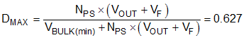
Because the maximum duty cycle exceeds 50%, and the design is an off-line (AC-input) application, the UCC28C42-Q1 is best suited for this application.