SLUSA12G December   2009  – November 2022 UCC28C40-Q1 , UCC28C41-Q1 , UCC28C42-Q1 , UCC28C43-Q1 , UCC28C44-Q1 , UCC28C45-Q1

PRODUCTION DATA  

  1. Features
  2. Applications
  3. Description
  4. Revision History
  5. Device Comparison Table
  6. Pin Configuration and Functions
  7. Specifications
    1. 7.1 Absolute Maximum Ratings
    2. 7.2 ESD Ratings
    3. 7.3 Recommended Operating Conditions
    4. 7.4 Thermal Information
    5. 7.5 Electrical Characteristics
    6. 7.6 Typical Characteristics
  8. Detailed Description
    1. 8.1 Overview
    2. 8.2 Functional Block Diagram
    3. 8.3 Feature Description
      1. 8.3.1  Detailed Pin Description
        1. 8.3.1.1 COMP
        2. 8.3.1.2 FB
        3. 8.3.1.3 CS
        4. 8.3.1.4 RT/CT
        5. 8.3.1.5 GND
        6. 8.3.1.6 OUT
        7. 8.3.1.7 VDD
        8. 8.3.1.8 VREF
      2. 8.3.2  Undervoltage Lockout
      3. 8.3.3  ±1% Internal Reference Voltage
      4. 8.3.4  Current Sense and Overcurrent Limit
      5. 8.3.5  Reduced-Discharge Current Variation
      6. 8.3.6  Oscillator Synchronization
      7. 8.3.7  Soft Start
      8. 8.3.8  Enable and Disable
      9. 8.3.9  Slope Compensation
      10. 8.3.10 Voltage Mode
    4. 8.4 Device Functional Modes
      1. 8.4.1 Normal Operation
      2. 8.4.2 UVLO Mode
  9. Application and Implementation
    1. 9.1 Application Information
    2. 9.2 Typical Application
      1. 9.2.1 Design Requirements
      2. 9.2.2 Detailed Design Procedure
        1. 9.2.2.1  Custom Design With WEBENCH® Tools
        2. 9.2.2.2  Input Bulk Capacitor and Minimum Bulk Voltage
        3. 9.2.2.3  Transformer Turns Ratio and Maximum Duty CycleG
        4. 9.2.2.4  Transformer Inductance and Peak Currents
        5. 9.2.2.5  Output Capacitor
        6. 9.2.2.6  Current Sensing Network
        7. 9.2.2.7  Gate Drive Resistor
        8. 9.2.2.8  VREF Capacitor
        9. 9.2.2.9  RT/CT
        10. 9.2.2.10 Start-Up Circuit
        11. 9.2.2.11 Voltage Feedback Compensation
          1. 9.2.2.11.1 Power Stage Poles and Zeroes
          2. 9.2.2.11.2 Slope Compensation
          3. 9.2.2.11.3 Open-Loop Gain
          4. 9.2.2.11.4 Compensation Loop
      3. 9.2.3 Application Curves
      4. 9.2.4 Power Supply Recommendations
      5. 9.2.5 Layout
        1. 9.2.5.1 Layout Guidelines
          1. 9.2.5.1.1 Precautions
          2. 9.2.5.1.2 Feedback Traces
          3. 9.2.5.1.3 Bypass Capacitors
          4. 9.2.5.1.4 Compensation Components
          5. 9.2.5.1.5 Traces and Ground Planes
        2. 9.2.5.2 Layout Example
  10. 10Device and Documentation Support
    1. 10.1 Device Support
      1. 10.1.1 Development Support
        1. 10.1.1.1 Custom Design With WEBENCH® Tools
    2. 10.2 Documentation Support
      1. 10.2.1 Related Documentation
    3. 10.3 Related Links
    4. 10.4 Support Resources
    5. 10.5 Trademarks
    6. 10.6 Electrostatic Discharge Caution
    7. 10.7 Glossary
  11. 11Mechanical, Packaging, and Orderable Information

Package Options

Mechanical Data (Package|Pins)
Thermal pad, mechanical data (Package|Pins)
Orderable Information

Application Information

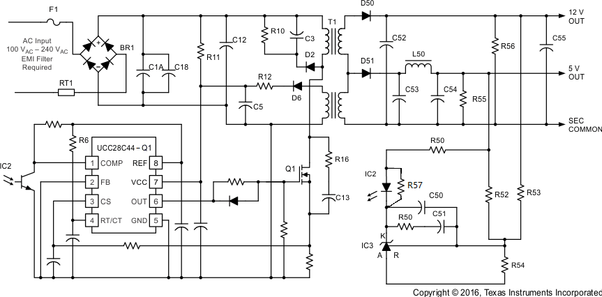
The UCC28C4x-Q1 controllers are peak current mode pulse width modulators. These controllers have an onboard amplifier and can be used in isolated and nonisolated power supply designs. There is an onboard totem pole gate driver capable of delivering 1 A of peak current. This is a high-speed PWM capable of operating at switching frequencies up to 1 MHz. Figure 9-1 shows a typical off-line application.
GUID-B21E7A00-8F43-4296-9324-EBEE0EC7744B-low.png Figure 9-1 Typical Off-Line Application