SLUS270G March 1999 – May 2020 UCC2800 , UCC2801 , UCC2802 , UCC2803 , UCC2804 , UCC2805
PRODUCTION DATA
- 1 Features
- 2 Applications
- 3 Description
- 4 Revision History
- 5 Description (continued)
- 6 Device Comparison Table
- 7 Pin Configuration and Functions
- 8 Specifications
-
9 Detailed Description
- 9.1 Overview
- 9.2 Functional Block Diagram
- 9.3
Feature Description
- 9.3.1 Detailed Pin Description
- 9.3.2 Undervoltage Lockout (UVLO)
- 9.3.3 Self-Biasing, Active Low Output
- 9.3.4 Reference Voltage
- 9.3.5 Oscillator
- 9.3.6 Synchronization
- 9.3.7 PWM Generator
- 9.3.8 Minimum Off-Time Setting (Dead-Time Control)
- 9.3.9 Leading Edge Blanking
- 9.3.10 Minimum Pulse Width
- 9.3.11 Current Limiting
- 9.3.12 Overcurrent Protection and Full Cycle Restart
- 9.3.13 Soft Start
- 9.3.14 Slope Compensation
- 9.4 Device Functional Modes
- 10Application and Implementation
- 11Power Supply Recommendations
- 12Layout
- 13Device and Documentation Support
- 14Mechanical, Packaging, and Orderable Information
Package Options
Mechanical Data (Package|Pins)
Thermal pad, mechanical data (Package|Pins)
Orderable Information
9.3.1.7 VCC
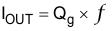
VCC is the power input connection for this device. In normal operation, VCC is powered through a current limiting resistor. Although quiescent VCC current is very low, total supply current is higher, depending on the OUT current. Total VCC current is the sum of quiescent VCC current and the average OUT current. Knowing the operating frequency and the MOSFET gate charge (Qg), average OUT current can be calculated from Equation 6.
The UCC280x has a lower VCC (supply voltage) clamp of 13.5 V typical versus 30 V on the UC3842. For applications that require a higher VCC voltage, a resistor must be placed in series with VCC to increase the source impedance. The maximum value of this resistor is calculated with Equation 7.
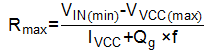
In Equation 7, VIN(min) is the minimum voltage that is used to supply VCC, VVCC(max) is the maximum VCC clamp voltage and IVCC is the IC supply current without considering the gate driver current and Qg is the external power MOSFET gate charge and f is the switching frequency.
Additionally, the UCC280x has an on-chip Zener diode to regulate VCC to 13.5 V. The turnon and turnoff thresholds for the UCC280x family are significantly different: 12.5 V and 8 V for the UCC2802 and UCC2804;
4.1 V and 3.6 V for the UCC2803 and UCC2805. 5-V PWM operation is now possible. To ensure against noise related problems, filter VCC with an electrolytic and bypass with a ceramic capacitor to ground. Keep the capacitors close to the IC pins.