SLUS270G March 1999 – May 2020 UCC2800 , UCC2801 , UCC2802 , UCC2803 , UCC2804 , UCC2805
PRODUCTION DATA
- 1 Features
- 2 Applications
- 3 Description
- 4 Revision History
- 5 Description (continued)
- 6 Device Comparison Table
- 7 Pin Configuration and Functions
- 8 Specifications
-
9 Detailed Description
- 9.1 Overview
- 9.2 Functional Block Diagram
- 9.3
Feature Description
- 9.3.1 Detailed Pin Description
- 9.3.2 Undervoltage Lockout (UVLO)
- 9.3.3 Self-Biasing, Active Low Output
- 9.3.4 Reference Voltage
- 9.3.5 Oscillator
- 9.3.6 Synchronization
- 9.3.7 PWM Generator
- 9.3.8 Minimum Off-Time Setting (Dead-Time Control)
- 9.3.9 Leading Edge Blanking
- 9.3.10 Minimum Pulse Width
- 9.3.11 Current Limiting
- 9.3.12 Overcurrent Protection and Full Cycle Restart
- 9.3.13 Soft Start
- 9.3.14 Slope Compensation
- 9.4 Device Functional Modes
- 10Application and Implementation
- 11Power Supply Recommendations
- 12Layout
- 13Device and Documentation Support
- 14Mechanical, Packaging, and Orderable Information
Package Options
Mechanical Data (Package|Pins)
Thermal pad, mechanical data (Package|Pins)
Orderable Information
9.3.13 Soft Start
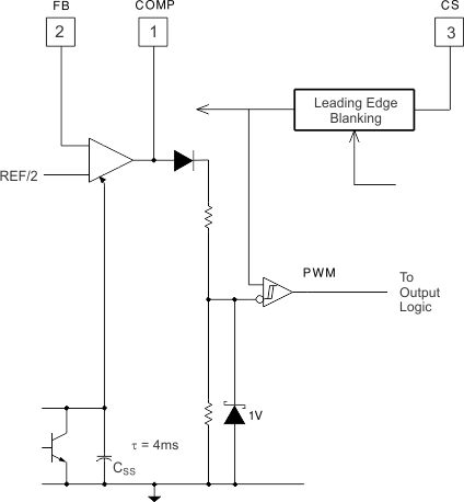
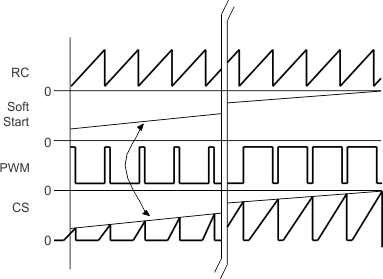
Internal soft starting of the PWM output is accomplished by gradually increasing error amplifier (E/A) output voltage. When used in current mode control, this implementation slowly raises the peak switch current each PWM cycle in comparison, forcing a controlled start-up. In voltage mode (duty cycle) control, this feature continually widens the pulse width.
 Figure 9-20 Detailed Block Diagram for Soft-Start
The internal soft-start capacitor (Css) is discharged following an undervoltage lockout transition or if the reference voltage is below a minimum value for normal operation. Additionally, discharge of Css occurs whenever the overcurrent protection comparator is triggered by a fault. Soft start is performed within the UCCx800, UCC2801, UCC2802, UCC2803, UCC2804, and UCC2805 devices by clamping the E/A amplifier output to an internal soft-start capacitor (Css), which is charged by a current source. The soft-start clamp circuitry is overridden once Css charges above the voltage commanded by the error amplifier for normal PWM operation.
 Figure 9-21 IC Soft-Start Behavior