SLUS456F April   1999  – July 2018 UCC2808A-1 , UCC2808A-2 , UCC3808A-1 , UCC3808A-2

PRODUCTION DATA.  

  1. Features
  2. Applications
  3. Description
    1.     Device Images
      1.      Simplified Application
  4. Revision History
  5. Pin Configuration and Functions
    1.     Pin Functions
  6. Specifications
    1. 6.1 Absolute Maximum Ratings
    2. 6.2 ESD Ratings
    3. 6.3 Recommended Operating Conditions
    4. 6.4 Thermal Information
    5. 6.5 Electrical Characteristics
    6. 6.6 Typical Characteristics
  7. Detailed Description
    1. 7.1 Overview
    2. 7.2 Functional Block Diagrams
    3. 7.3 Feature Description
      1. 7.3.1 Pin Descriptions
        1. 7.3.1.1 COMP
        2. 7.3.1.2 CS
        3. 7.3.1.3 FB
        4. 7.3.1.4 GND
        5. 7.3.1.5 OUTA and OUTB
        6. 7.3.1.6 RC
        7. 7.3.1.7 VDD
    4. 7.4 Device Functional Modes
      1. 7.4.1 VCC
      2. 7.4.2 Push-Pull or Half-Bridge Function
  8. Application and Implementation
    1. 8.1 Application Information
    2. 8.2 Typical Application
      1. 8.2.1 Design Requirements
      2. 8.2.2 Detailed Design Procedure
      3. 8.2.3 Application Curves
  9. Power Supply Recommendations
  10. 10Layout
    1. 10.1 Layout Guidelines
    2. 10.2 Layout Example
  11. 11Device and Documentation Support
    1. 11.1 Documentation Support
      1. 11.1.1 Related Documentation
    2. 11.2 Related Links
    3. 11.3 Receiving Notification of Documentation Updates
    4. 11.4 Community Resources
    5. 11.5 Trademarks
    6. 11.6 Electrostatic Discharge Caution
    7. 11.7 Glossary
  12. 12Mechanical, Packaging, and Orderable Information

Package Options

Refer to the PDF data sheet for device specific package drawings

Mechanical Data (Package|Pins)
  • D|8
  • PW|8
Thermal pad, mechanical data (Package|Pins)
Orderable Information

Typical Characteristics

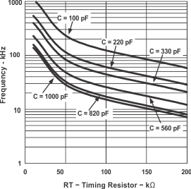
UCC2808A-1 UCC2808A-2 UCC3808A-1 UCC3808A-2 graph_01_slus456.gifFigure 1. Oscillator Frequency
vs External RC Values
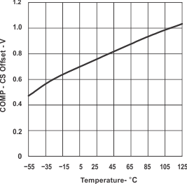
UCC2808A-1 UCC2808A-2 UCC3808A-1 UCC3808A-2 graph_03_slus456.gifFigure 3. COMP to CS Offset vs Temperature
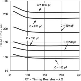
UCC2808A-1 UCC2808A-2 UCC3808A-1 UCC3808A-2 graph_05_slus456.gifFigure 5. Output Dead Time vs External RC Values
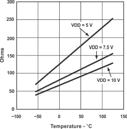
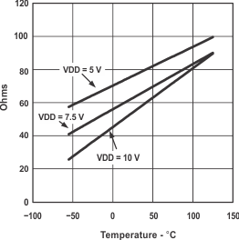
UCC2808A-1 UCC2808A-2 UCC3808A-1 UCC3808A-2 graph_07_slus456.gifFigure 7. RC RDS(on) vs Temperature
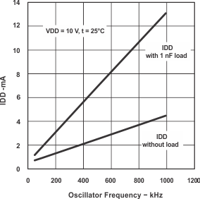
UCC2808A-1 UCC2808A-2 UCC3808A-1 UCC3808A-2 graph_02_slus456.gifFigure 2. IDD vs Oscillator Frequency
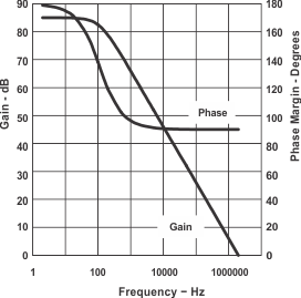
UCC2808A-1 UCC2808A-2 UCC3808A-1 UCC3808A-2 graph_04_slus456.gifFigure 4. Error Amplifier Gain and Phase Response
vs Frequency
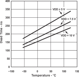
UCC2808A-1 UCC2808A-2 UCC3808A-1 UCC3808A-2 graph_06_slus456.gifFigure 6. Dead Time vs Temperature
UCC2808A-1 UCC2808A-2 UCC3808A-1 UCC3808A-2 graph_08_slus456.gifFigure 8. CS RDS(on) vs Temperature