SLUSB72D March   2013  – April 2021 UCD3138064

PRODUCTION DATA  

  1. Features
  2. Applications
  3. Description
  4. Functional Block Diagram
  5. Revision History
  6. Device Options
    1. 6.1 Device Comparison Table
    2. 6.2 Product Selection Matrix
  7. Pin Configuration and Functions
    1. 7.1 Pin Diagrams
    2. 7.2 Pin Functions
  8. Specifications
    1. 8.1  Absolute Maximum Ratings (1)
    2. 8.2  Handling Ratings
    3. 8.3  Recommended Operating Conditions
    4. 8.4  Thermal Information
    5. 8.5  Electrical Characteristics
    6. 8.6  Timing Characteristics
    7. 8.7  PMBus/SMBus/I2C Timing
    8. 8.8  Power On Reset (POR) / Brown Out Reset (BOR)
    9. 8.9  Typical Clock Gating Power Savings
    10. 8.10 Typical Characteristics
  9. Detailed Description
    1. 9.1 Overview
      1. 9.1.1 ARM Processor
      2. 9.1.2 Memory
    2. 9.2 Functional Block Diagram
    3. 9.3 Feature Description
      1. 9.3.1  System Module
        1. 9.3.1.1 Address Decoder (DEC)
        2. 9.3.1.2 Memory Management Controller (MMC)
        3. 9.3.1.3 System Management (SYS)
        4. 9.3.1.4 Central Interrupt Module (CIM)
      2. 9.3.2  Peripherals
        1. 9.3.2.1 Digital Power Peripherals
          1. 9.3.2.1.1 Front End
          2. 9.3.2.1.2 DPWM Module
          3. 9.3.2.1.3 DPWM Events
          4. 9.3.2.1.4 High Resolution DPWM
          5. 9.3.2.1.5 Over Sampling
          6. 9.3.2.1.6 DPWM Interrupt Generation
          7. 9.3.2.1.7 DPWM Interrupt Scaling/Range
      3. 9.3.3  Automatic Mode Switching
        1. 9.3.3.1 Phase Shifted Full Bridge Example
        2. 9.3.3.2 LLC Example
        3. 9.3.3.3 Mechanism For Automatic Mode Switching
      4. 9.3.4  DPWMC, Edge Generation, Intramux
      5. 9.3.5  Filter
        1. 9.3.5.1 Loop Multiplexer
        2. 9.3.5.2 Fault Multiplexer
      6. 9.3.6  Communication Ports
        1. 9.3.6.1 SCI (UART) Serial Communication Interface
        2. 9.3.6.2 PMBUS/I2C
        3. 9.3.6.3 SPI
      7. 9.3.7  Real Time Clock
      8. 9.3.8  Timers
        1. 9.3.8.1 24-Bit Timer
        2. 9.3.8.2 16-Bit PWM Timers
        3. 9.3.8.3 Watchdog Timer
      9. 9.3.9  General Purpose ADC12
      10. 9.3.10 Miscellaneous Analog
      11. 9.3.11 Brownout
      12. 9.3.12 Global I/O
      13. 9.3.13 Temperature Sensor Control
      14. 9.3.14 I/O Mux Control
      15. 9.3.15 Current Sharing Control
      16. 9.3.16 Temperature Reference
    4. 9.4 Device Functional Modes
      1. 9.4.1 DPWM Modes Of Operation
        1. 9.4.1.1 Normal Mode
        2. 9.4.1.2 Phase Shifting
        3. 9.4.1.3 DPWM Multiple Output Mode
        4. 9.4.1.4 DPWM Resonant Mode
      2. 9.4.2 Triangular Mode
      3. 9.4.3 Leading Edge Mode
    5. 9.5 Memory
      1. 9.5.1 Register Maps
        1. 9.5.1.1 CPU Memory Map and Interrupts
          1. 9.5.1.1.1 Memory Map (After Reset Operation)
          2. 9.5.1.1.2 Memory Map (Normal Operation)
          3. 9.5.1.1.3 Memory Map (System and Peripherals Blocks)
        2. 9.5.1.2 Boot ROM
        3. 9.5.1.3 Customer Boot Program
        4. 9.5.1.4 Flash Management
        5. 9.5.1.5 Synchronous Rectifier MOSFET Ramp and IDE Calculation
  10. 10Applications and Implementation
    1. 10.1 Application Information
    2. 10.2 Typical Application
      1. 10.2.1 Design Requirements
      2. 10.2.2 Detailed Design Procedure
        1. 10.2.2.1 PCMC (Peak Current Mode Control) PSFB (Phase Shifted Full Bridge) Hardware Configuration Overview
        2. 10.2.2.2 DPWM Initialization for PSFB
          1. 10.2.2.2.1 DPWM Synchronization
        3. 10.2.2.3 Fixed Signals to Bridge
        4. 10.2.2.4 Dynamic Signals to Bridge
        5. 10.2.2.5 System Initialization for PCM
          1. 10.2.2.5.1 Use of Front Ends and Filters in PSFB
          2. 10.2.2.5.2 Peak Current Detection
          3. 10.2.2.5.3 Peak Current Mode (PCM)
      3. 10.2.3 Application Curves
  11. 11Power Supply Recommendations
    1. 11.1 Introduction To Power Supply and Layout Recommendations
    2. 11.2 3.3-V Supply Pins
    3. 11.3 Recommendation for V33 Ramp up Slew Rate for UCD3138 and UCD3138064
    4. 11.4 Recommendation for RC Time Constant of RESET Pin for UCD3138 and UCD3138064
  12. 12Layout
    1. 12.1 Layout Guidelines
      1. 12.1.1 EMI and EMC Mitigation Guidelines
      2. 12.1.2 BP18 Pin
      3. 12.1.3 Additional Bias Guidelines
      4. 12.1.4 UART Communication Port
    2. 12.2 Layout Example
      1. 12.2.1 UCD3138 and UCD3138064 40 Pin
      2. 12.2.2 UCD3138 and UCD3138064 64 Pin
  13. 13Device and Documentation Support
    1. 13.1 Device Support
    2. 13.2 Documentation Support
      1. 13.2.1 Related Documentation
    3. 13.3 Trademarks
    4. 13.4 Electrostatic Discharge Caution
    5. 13.5 Glossary
  14. 14Mechanical, Packaging, and Orderable Information

Package Options

Mechanical Data (Package|Pins)
Thermal pad, mechanical data (Package|Pins)
Orderable Information

Fixed Signals to Bridge

The two top signals in the above drawing have fixed timing. The DPWM1CF and DPWM2CF signals are used for these pins. DPWMCxF refers to the signal coming out of the fault module of DPWMx, as shown in Figure 10-4.
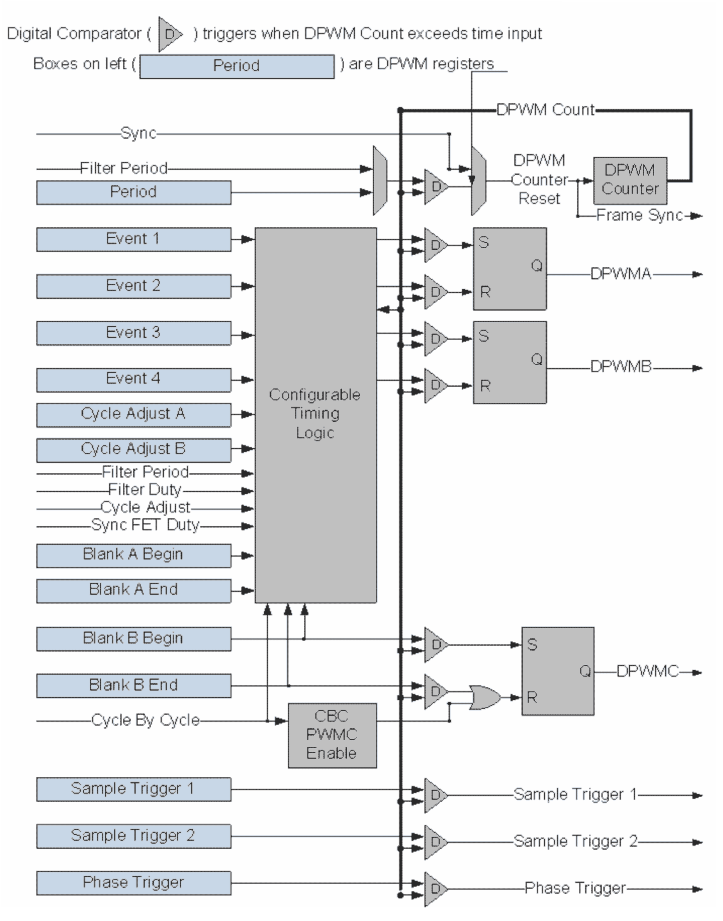
GUID-9BC07F5E-5A1F-443D-8AFA-F38DFA926DDF-low.gifFigure 10-4 Fixed Signals to Bridge

These signals are actually routed to pins DPWM3A and 3B using the Intra Mux with these statements:

Dpwm3Regs.DPWMCTRL0.bit.PWM_A_INTRA_MUX = 7; // Send DPWM1C
Dpwm3Regs.DPWMCTRL0.bit.PWM_B_INTRA_MUX = 8; // Send DPWM2C

Since these signals are really being used as events in the timer, the #defines are called EV5 and EV6. Here are the statements which initialize them:

// Setup waveform for DPWM-C (re-using blanking B regs)
Dpwm2Regs.DPWMBLKBBEG.all = PWM2_EV5 + (4 *16);
Dpwm2Regs.DPWMBLKBEND.all = PWM2_EV6;
GUID-4AD24F8A-73EE-4939-8D87-7C03A25B626F-low.gifFigure 10-5 Blank B Timing Information

The statements for DPWM1 are the same. Remember that DPWMC reuses the Blank B registers for timing information.