SLUSB72D March 2013 – April 2021 UCD3138064
PRODUCTION DATA
- 1 Features
- 2 Applications
- 3 Description
- 4 Functional Block Diagram
- 5 Revision History
- 6 Device Options
- 7 Pin Configuration and Functions
-
8 Specifications
- 8.1 Absolute Maximum Ratings (1)
- 8.2 Handling Ratings
- 8.3 Recommended Operating Conditions
- 8.4 Thermal Information
- 8.5 Electrical Characteristics
- 8.6 Timing Characteristics
- 8.7 PMBus/SMBus/I2C Timing
- 8.8 Power On Reset (POR) / Brown Out Reset (BOR)
- 8.9 Typical Clock Gating Power Savings
- 8.10 Typical Characteristics
-
9 Detailed Description
- 9.1 Overview
- 9.2 Functional Block Diagram
- 9.3
Feature Description
- 9.3.1 System Module
- 9.3.2 Peripherals
- 9.3.3 Automatic Mode Switching
- 9.3.4 DPWMC, Edge Generation, Intramux
- 9.3.5 Filter
- 9.3.6 Communication Ports
- 9.3.7 Real Time Clock
- 9.3.8 Timers
- 9.3.9 General Purpose ADC12
- 9.3.10 Miscellaneous Analog
- 9.3.11 Brownout
- 9.3.12 Global I/O
- 9.3.13 Temperature Sensor Control
- 9.3.14 I/O Mux Control
- 9.3.15 Current Sharing Control
- 9.3.16 Temperature Reference
- 9.4 Device Functional Modes
- 9.5 Memory
-
10Applications and
Implementation
- 10.1 Application Information
- 10.2
Typical Application
- 10.2.1 Design Requirements
- 10.2.2 Detailed Design Procedure
- 10.2.3 Application Curves
- 11Power Supply Recommendations
- 12Layout
- 13Device and Documentation Support
- 14Mechanical, Packaging, and Orderable Information
Package Options
Mechanical Data (Package|Pins)
Thermal pad, mechanical data (Package|Pins)
Orderable Information
9.3.9 General Purpose ADC12
The ADC12 is a 12 bit, high speed analog to digital converter, equipped with the following options:
- Typical conversion speed of 267 ksps
- Conversions can consist from 1 to 16 ADC channel conversions in any desired sequence
- Post conversion averaging capability, ranging from 4X, 8X, 16X or 32X samples
- Configurable triggering for ADC conversions from the following sources: firmware, DPWM rising edge, ADC_EXT_TRIG pin or Analog Comparator results
- Interrupt capability to embedded processor at completion of ADC conversion
- Six digital comparators on the first 6 channels of the conversion sequence using either raw ADC data or averaged ADC data
- Two 10 µA current sources for excitation of PMBus addressing resistors
- Dual sample and hold for accurate power measurement
- Internal temperature sensor for temperature protection and monitoring
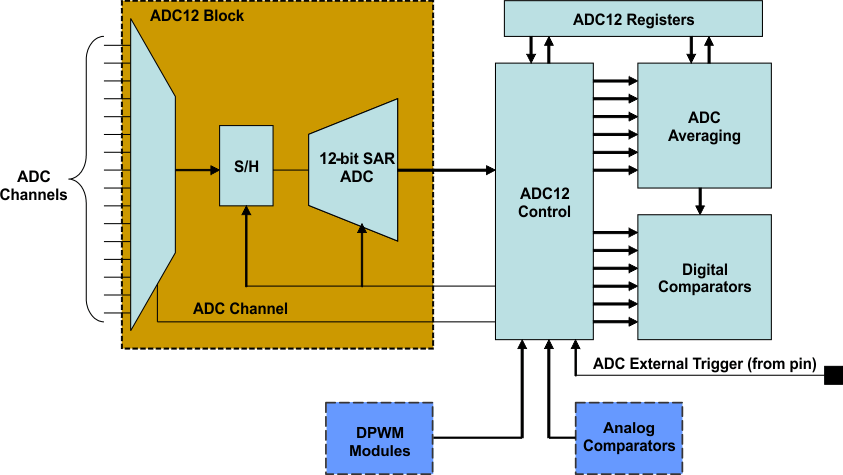
The control module (Figure 9-19) contains the control and conversion logic for auto-sequencing a series of conversions. The sequencing is fully configurable for any combination of 16 possible ADC channels through an analog multiplexer embedded in the ADC12 block. Once converted, the selected channel value is stored in the result register associated with the sequence number. Input channels can be sampled in any desired order or programmed to repeat conversions on the same channel multiple times during a conversion sequence. Selected channel conversions are also stored in the result registers in order of conversion, where the result 0 register is the first conversion of a 16-channel sequence and result 15 register is the last conversion of a 16-channel sequence. The number of channels converted in a sequence can vary from 1 to 16.
Unlike EADC0 through EADC2, which are primarily designed for closing high speed compensation loops, the ADC12 is not usually used for loop compensation purposes. The EADC converters have a substantially faster conversion rate, thus making them more attractive for closed loop control. The ADC12 features make it best suited for monitoring and detection of currents, voltages, temperatures and faults. Please see the Section 8.10 for the temperature variation associated with this function.
 Figure 9-19 ADC12 Control Block Diagram