SLUSCA5B December 2015 – January 2017 UCD3138064A
PRODUCTION DATA.
- 1Device Overview
- 2Revision History
- 3Device Options
- 4Pin Configuration and Functions
- 5Specifications
-
6Detailed Description
- 6.1 Overview
- 6.2 ARM Processor
- 6.3 Memory
- 6.4
Feature Description
- 6.4.1 System Module
- 6.4.2 Peripherals
- 6.4.3 Synchronous Rectifier Dead Time Optimization Peripheral
- 6.4.4 Automatic Mode Switching
- 6.4.5 DPWMC, Edge Generation, IntraMux
- 6.4.6 Filter
- 6.4.7 Communication Ports
- 6.4.8 Timers
- 6.4.9 General Purpose ADC12
- 6.4.10 Miscellaneous Analog
- 6.4.11 Brownout
- 6.4.12 Global I/O
- 6.4.13 Temperature Sensor Control
- 6.4.14 I/O Mux Control
- 6.4.15 Current Sharing Control
- 6.4.16 Temperature Reference
- 6.5 Device Functional Modes
- 6.6 Memory
-
7Applications, Implementation, and Layout
- 7.1 Application Information
- 7.2
Typical Application
- 7.2.1 Design Requirements
- 7.2.2 Detailed Design Procedure
- 7.2.3 Application Curves
- 7.2.4 Power Supply Recommendations
- 7.2.5 Layout
- 8Device and Documentation Support
- 9Mechanical, Packaging, and Orderable Information
Package Options
Mechanical Data (Package|Pins)
- RGC|64
Thermal pad, mechanical data (Package|Pins)
- RGC|64
Orderable Information
5 Specifications
5.1 Absolute Maximum Ratings
over operating free-air temperature range (unless otherwise noted) (1)| MIN | MAX | UNIT | ||
|---|---|---|---|---|
| V33D | V33D to DGND | –0.3 | 3.8 | V |
| V33DIO | V33DIO to DGND | –0.3 | 3.8 | V |
| V33A | V33A to AGND | –0.3 | 3.8 | V |
| BP18 | BP18 to DGND | –0.3 | 2.5 | V |
| Ground difference | |DGND – AGND| | 0.3 | V | |
| All Pins, excluding AGND (2) | Voltage applied to any pin | –0.3 | 3.8 | V |
| Junction Temperature, TJ | –40 | 125 | °C | |
| Storage temperature, Tstg | –55 | 150 | ||
5.2 ESD Ratings
| VALUE | UNIT | ||||
|---|---|---|---|---|---|
| V(ESD) | Electrostatic discharge | Human-body model (HBM), per ANSI/ESDA/JEDEC JS-001 (1) | ±2000 | V | |
| Charged-device model (CDM), per JEDEC specification JESD22-C101 (2) | ±500 | ||||
5.3 Recommended Operating Conditions
over operating free-air temperature range (unless otherwise noted)| MIN | NOM | MAX | UNIT | ||
|---|---|---|---|---|---|
| V33D | Digital power | 3 | 3.3 | 3.6 | V |
| V33DIO | Digital I/O power | 3 | 3.3 | 3.6 | V |
| V33A | Analog power | 3 | 3.3 | 3.6 | V |
| BP18 | 1.8-V digital power | 1.6 | 1.8 | 2 | V |
| TJ | Junction temperature | –40 | - | 125 | °C |
5.4 Thermal Information
| THERMAL METRIC (1) | UCD3138064A | UNIT | |
|---|---|---|---|
| VQFN (RGC) | |||
| 64 PINS | |||
| RθJA | Junction-to-ambient thermal resistance | 19.9 | °C/W |
| RθJC(top) | Junction-to-case (top) thermal resistance | 5.7 | °C/W |
| RθJB | Junction-to-board thermal resistance | 3.1 | °C/W |
| ψJT | Junction-to-top characterization parameter | 0.1 | °C/W |
| ψJB | Junction-to-board characterization parameter | 3 | °C/W |
| RθJC(bot) | Junction-to-case (bottom) thermal resistance | 0.3 | °C/W |
5.5 Electrical Characteristics
V33A = V33D = V33DIO = 3V to 3.6 V; 1μF from BP18 to DGND, TJ = –40 °C to 125 °C (unless otherwise noted)| PARAMETER | TEST CONDITIONS | MIN | TYP | MAX | UNIT | |
|---|---|---|---|---|---|---|
| SUPPLY CURRENT | ||||||
| I33A | Measured on V33A. The device is powered up but all ADC12 and EADC sampling is disabled | 6.3 | mA | |||
| I33DIO | All GPIO and communication pins are open | 0.35 | mA | |||
| I33D | ROM program execution | 60 | mA | |||
| I33D (4) | Flash programming in ROM mode | 70 | mA | |||
| I33 | The device is in ROM mode with all DPWMs enabled and switching at 2 MHz. The DPWMs are all unloaded. | 105 | mA | |||
| ERROR ADC INPUTS EAP, EAN | ||||||
| EAP – AGND | –0.15 | 1.998 | V | |||
| EAP – EAN | –0.256 | 1.848 | V | |||
| Typical error range | AFE = 0 | –256 | 248 | mV | ||
| EAP – EAN Error voltage digital resolution | AFE = 3 | 0.8 | 1 | 1.20 | mV | |
| AFE = 2 | 1.7 | 2 | 2.30 | mV | ||
| AFE = 1 | 3.55 | 4 | 4.45 | mV | ||
| AFE = 0 | 6.90 | 8 | 9.10 | mV | ||
| REA (4) | Input impedance (See Figure 6-2) | AGND reference | 0.5 | MΩ | ||
| IOFFSET | Input offset current (See Figure 6-2) | –5 | 5 | μA | ||
| EADC Offset | Input voltage = 0 V at AFE = 0 | –2 | 2 | LSB | ||
| Input voltage = 0 V at AFE = 1 | –2.5 | 2.5 | LSB | |||
| Input voltage = 0 V at AFE = 2 | –3 | 3 | LSB | |||
| Input voltage = 0 V at AFE = 3 | –4 | 4 | LSB | |||
| Sample Rate | 15.625 | MHz | ||||
| Analog Front End Amplifier Bandwidth (4) | 100 | MHz | ||||
| A0 | Gain | See Figure 6-3 | 1 | V/V | ||
| Minimum output voltage | 21 | mV | ||||
| EADC DAC | ||||||
| DAC range | 0 | 1.6 | V | |||
| VREF DAC reference resolution | 10-bit, No dithering enabled | 1.56 | mV | |||
| VREF DAC reference resolution | With 4-bit dithering enabled | 97.6 | μV | |||
| INL | –2.0 | 2.0 | LSB | |||
| DNL | –2.0 | 2.0 | LSB | |||
| DAC reference voltage | 1.58 | 1.61 | V | |||
| τ | Settling Time (4) | From 10% to 90% | 250 | ns | ||
| ADC12 | ||||||
| IBIAS | Bias current for PMBus address pins | 9.5 | 10.5 | μA | ||
| Measurement range for voltage monitoring | 0 | 2.5 | V | |||
| Internal ADC reference voltage | –40 to 125 °C | 2.475 | 2.500 | 2.53 | V | |
| Change in Internal ADC reference from 25°C reference voltage (4) | –40 to 25 °C | –0.3 | mV | |||
| 25 to 125 °C | –3.4 | |||||
| ADC12 INL integral nonlinearity, end point (4) | ADC_SAMPLING_SEL = 6 for all ADC12 data, 25 to 125 °C | –3.9 | –2/+2 | 4.5 | LSB | |
| ADC12 INL integral nonlinearity, best fit | –2.4 | –1.5/+1.5 | 2.9 | LSB | ||
| ADC12 DNL differential nonlinearity (4) | –0.8/+2.9 | LSB | ||||
| ADC Zero Scale Error | –7 | 7 | mV | |||
| ADC Full Scale Error | –35 | 35 | mV | |||
| Input bias | 2.5 V applied to pin | 200 | nA | |||
| Input leakage resistance (4) | ADC_SAMPLING_SEL= 6 or 0 | 1 | MΩ | |||
| Input Capacitance (4) | 10 | pF | ||||
| ADC single sample conversion time | 3.744 | μs | ||||
| DIGITAL INPUTS/OUTPUTS (1) | ||||||
| VOL | Low-level output voltage (2) | IOH = 4 mA, V33DIO = 3 V | DGND + 0.25 |
V | ||
| VOH | High-level output voltage (2) | IOH = –4 mA, V33DIO = 3 V | V33DIO – 0.6 | V | ||
| VIH | High-level input voltage | V33DIO = 3 V | 2.1 | V | ||
| VIL | Low-level input voltage | V33DIO = 3 V | 1.1 | V | ||
| IOH | Output sinking current | 4 | mA | |||
| IOL | Output sourcing current | –4 | mA | |||
| VOL(PMBus) | Low-level output voltage for PMBus pins (PMBUS_CLK, PMBUS_DATA, PMBUS_ALERT, PMBUS_CTRL) | IOL = 20 mA | 400 | mV | ||
| SYSTEM PERFORMANCE | ||||||
| tWD | Watchdog timeout resolution | 13.1 | 17 | 22.7 | ms | |
| Processor master clock (MCLK) | 31.25 | MHz | ||||
| tDelay | Digital filter delay (3) | (1 clock = 32 ns) | 6 | MCLKs | ||
| Retention period of flash content (data retention and program) | TJ = 25 °C | 100 | years | |||
| f(PCLK) | Internal oscillator frequency | –40 C to +125 C | 240 | 250 | 260 | MHz |
| –5 C to +85 C | 245 | 250 | 255 | MHz | ||
| f(LFO) | Internal low frequency oscillator frequency | 10 | MHz | |||
| Flash Read | 1 | MCLKs | ||||
| ISHARE | Current share current source (See Figure 6-25) | 238 | 259 | μA | ||
| RSHARE | Current share resistor (See Figure 6-25) | 9.75 | 10.3 | kΩ | ||
| POWER ON RESET AND BROWN OUT (V33A PIN, SEE Figure 5-4) | ||||||
| VGH | Voltage Good High | 2.6 | V | |||
| VGL | Voltage Good Low | 2.55 | V | |||
| Vres (4) | Voltage at which IReset signal is valid(4) | 0.8 | V | |||
| Brownout | Internal signal warning of brownout conditions | 2.9 | V | |||
| TEMPERATURE SENSOR (4) | ||||||
| VTEMP | Voltage range of sensor | 1.46 | 2.44 | V | ||
| Voltage resolution | Volts/°C | 5.9 | mV/ºC | |||
| Temperature resolution | Degree C per bit | 0.1034 | ºC/LSB | |||
| Accuracy (4) (5) | –40 to 125 °C | –10 | ±5 | 10 | ºC | |
| Temperature range | –40 to 125 °C | –40 | 125 | ºC | ||
| ITEMP | Current draw of sensor when active | 30 | μA | |||
| VAMB | Ambient temperature | Trimmed 25 °C reading | 1.85 | V | ||
| ANALOG COMPARATOR | ||||||
| DAC | Reference DAC Range | 0.01953 | 2.5 | V | ||
| Reference Voltage | 2.478 | 2.5 | 2.513 | V | ||
| Bits | 7 | bits | ||||
| INL (4) | –0.5 | 0.21 | LSB | |||
| DNL (4) | 0.06 | 0.12 | LSB | |||
| Offset (4) | –19.5 | 19.5 | mV | |||
| Reference DAC buffered output load (6) | –0.5 | 1 | mA | |||
| Buffer Offset (–0.5 mA) | 0.156V < DAC < 2.363V | –10 | 10 | mV | ||
| Buffer Offset (1.0 mA) | 0.059V < DAC < 2.305V | –10 | 10 | mV | ||
5.6 Timing Characteristics
V33A = V33D = V33DIO = 3.3 V; 1 μF from BP18 to DGND, TJ = –40 to 125 °C (unless otherwise noted)| PARAMETER | TEST CONDITION | MIN | TYP | MAX | UNIT | |
|---|---|---|---|---|---|---|
| EADC DAC | ||||||
| τ | Settling Time | From 10 to 90% | 250 | ns | ||
| ADC12 | ||||||
| ADC single sample conversion time (1) | ADC_SAMPLING_SEL= 6 or 0 | 3.9 | μs | |||
| SYSTEM PERFORMANCE | ||||||
| Time to disable DPWM output based on active FAULT pin signal | High level on FAULT pin | 70 | ns | |||
| Retention period of flash content (data retention and program) | TJ = 25 °C | 100 | years | |||
| Program time to erase one page or block in data flash or program flash | 20 | ms | ||||
| Program time to write one word in data flash or program flash | 30 | µs | ||||
| Sync-in/sync-out pulse width | Sync pin | 256 | ns | |||
| Flash Write | 20 | μs | ||||
| POWER ON RESET AND BROWN OUT (V33D PIN, SEE Figure 5-4 | ||||||
| tPOR | Time delay after Power is good or RESET* relinquished | 1 | ms | |||
| tEXC1 | The time it takes from the device to exit a reset state and begin executing program flash bank 1 (32 kB). (1) | IRESET goes from a low state to a high state. This is approximately equivalent to toggling the external reset pin from low to high state. | 9.5 | ms | ||
| tEXC2 | The time it takes from the device to exit a reset state and begin executing program flash bank 2 (32 kB). (1) | IRESET goes from a low state to a high state. This is approximately equivalent to toggling the external reset pin from low to high state. | 19 | ms | ||
| tEXCT | The time it takes from the device to exit a reset state and begin executing the total program flash (64 kB). (1) | IRESET goes from a low state to a high state. This is approximately equivalent to toggling the external reset pin from low to high state. | 19 | ms | ||
| TEMPERATURE SENSOR (1) | ||||||
| tON | Turn on time / settling time of sensor | 100 | μs | |||
| ANALOG COMPARATOR | ||||||
| Time to disable DPWM output based on 0 V to 2.5 V step input on the analog comparator. (1) | 150 | ns | ||||
5.7 PMBus/SMBus/I2C Timing
The timing characteristics and timing diagram for the communications interface that supports I2C, SMBus, and PMBus in Slave or Master mode are shown in Table 5-1, Figure 5-1, and Figure 5-2. The numbers in Table 5-1 shows that the device supports standard (100 kHz), fast (400 kHz), and fast-mode plus (1 MHz) speeds.
Table 5-1 I2C/SMBus/PMBus Timing Characteristics
| PARAMETER | TEST CONDITIONS | 100 kHz Class | 400 kHz Class | 1 MHz Class | UNIT | ||||
|---|---|---|---|---|---|---|---|---|---|
| MIN | MAX | MIN | MAX | MIN | MAX | ||||
| Typical values at TA = 25 °C and VCC = 3.3 V (unless otherwise noted) | |||||||||
| fSMB | SMBus/PMBus operating frequency | Slave mode, SMBC 50% duty cycle | 10 | 100 | 10 | 400 | 10 | 1000 | kHz |
| fI2C | I2C operating frequency | Slave mode, SCL 50% duty cycle | 10 | 100 | 10 | 400 | 10 | 1000 | kHz |
| t(BUF) | Bus free time between start and stop(1) | 4.7 | 1.3 | 0.5 | µs | ||||
| t(HD:STA) | Hold time after (repeated) start(1) | 4 | 0.6 | 0.26 | µs | ||||
| t(SU:STA) | Repeated start setup time(1) | 4.7 | 0.6 | 0.26 | µs | ||||
| t(SU:STO) | Stop setup time(1) | 4 | 0.6 | 0.26 | µs | ||||
| t(HD:DAT) | Data hold time | Receive mode | 0 | 0 | 0 | ns | |||
| t(SU:DAT) | Data setup time | 250 | 100 | 50 | ns | ||||
| t(TIMEOUT) | Error signal/detect(2) | 25 | 35 | 25 | 35 | 25 | 35 | ms | |
| t(LOW) | Clock low period | 4.7 | 1.3 | 0.5 | µs | ||||
| t(HIGH) | Clock high period(3) | 4 | 50 | 0.6 | 50 | 0.26 | 50 | µs | |
| t(LOW:SEXT) | Cumulative clock low slave extend time(4) | 25 | 25 | 25 | ms | ||||
| tr | Clock/data fall time | Rise time tr = (VILmax – 0.15) to (VIHmin + 0.15) | 20 + 0.1 Cb(5) |
300 | 20 + 0.1 Cb(5) |
300 | 20 + 0.1 Cb(5) |
120 | ns |
| tf | Clock/data rise time | Fall time tf = 0.9 VDD to (VILmax – 0.15) | 20 + 0.1 Cb(5) |
1000 | 20 + 0.1 Cb(5) |
300 | 20 + 0.1 Cb(5) |
120 | ns |
| Cb | Total capacitance of one bus line | 400 | pF | ||||||
 Figure 5-1 I2C/SMBus/PMBus Timing Diagram
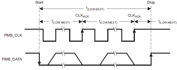 Figure 5-2 Bus Timing in Extended Mode
5.8 Parametric Measurement Information
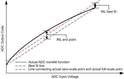 Figure 5-3 Best Fit INL and End Point INL
 Figure 5-4 Power On Reset (POR) / Brown Out Reset (BOR)
| VGH | – | This is the V33A threshold where the internal power is declared good. The UCD3138064A comes out of reset when above this threshold. |
| VGL | – | This is the V33A threshold where the internal power is declared bad. The device goes into reset when below this threshold. |
| Vres | – | This is the V33A threshold where the internal reset signal is no longer valid. Below this threshold the device is in an indeterminate state. |
| IReset | – | This is the internal reset signal. When low, the device is held in reset. This is equivalent to holding the reset pin on the IC low. |
| TPOR | – | The time delay from when VGH is exceeded to when the device comes out of reset. |
| Brown Out | – | This is the V33A voltage threshold at which the device sets the brown out status bit. In addition an interrupt can be triggered if enabled. |
5.9 Typical Characteristics
(Data is taken from the UCD3138)
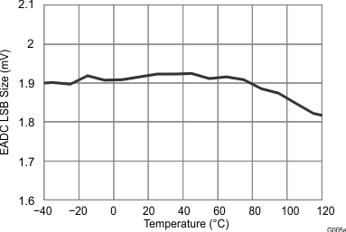 Figure 5-5 EADC LSB Size with 4X Gain (mV) vs Temperature
 Figure 5-7 ADC12 2.5-V Reference vs Temperature
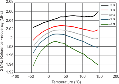 Figure 5-9 Oscillator Frequency (2MHz Reference, Divided Down from 250MHz) vs Temperature
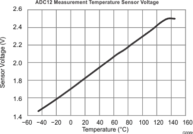 Figure 5-6 ADC12 Measurement Temperature Sensor Voltage vs Temperature
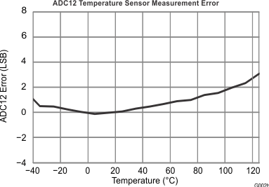 Figure 5-8 ADC12 Temperature Sensor Measurement Error vs Temperature
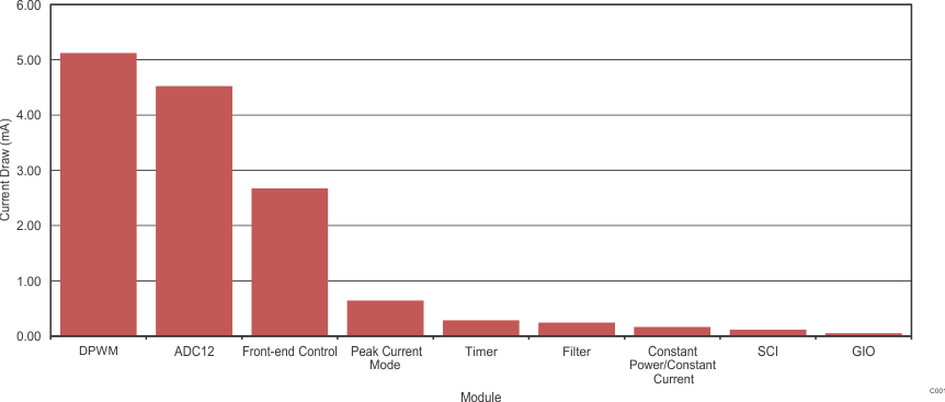 Figure 5-10 Clock Gating Power Savings
The power disable control register provides control bits that can enable or disable the clock to several peripherals such as, PCM, CPCC, digital filters, front ends, DPWMs, UARTs, ADC-12 and more.
By default, all these controls are enabled. If a specific peripheral is not used the clock gate can be disabled in order to block the propagation of the clock signal to that peripheral and therefore reduce the overall current consumption of the device. The power savings chart displays the power savings per module. For example there are 4 DPWM modules, therefore, if all 4 are disabled a total of ~20 mA can be saved.