SLVSDD4C September 2016 – March 2020 UCD90160A
PRODUCTION DATA.
- 1 Features
- 2 Applications
- 3 Description
- 4 Revision History
- 5 Pin Configuration and Functions
- 6 Specifications
-
7 Detailed Description
- 7.1 Overview
- 7.2 Functional Block Diagram
- 7.3 Feature Description
- 7.4
Device Functional Modes
- 7.4.1 Power Supply Sequencing
- 7.4.2 Pin-Selected Rail States
- 7.4.3 Voltage Monitoring
- 7.4.4 Fault Responses and Alert Processing
- 7.4.5 Shut Down All Rails and Sequence On (Resequence)
- 7.4.6 GPIOs
- 7.4.7 GPO Control
- 7.4.8 GPO Dependencies
- 7.4.9 GPI Special Functions
- 7.4.10 Power Supply Enables
- 7.4.11 Cascading Multiple Devices
- 7.4.12 PWM Outputs
- 7.4.13 Programmable Multiphase PWMs
- 7.4.14 Margining
- 7.4.15 System Reset Signal
- 7.4.16 Watch Dog Timer
- 7.4.17 Run Time Clock
- 7.4.18 Data and Error Logging to Flash Memory
- 7.4.19 Brownout Function
- 7.4.20 PMBus Address Selection
- 7.4.21 Device Reset
- 7.5 Programming
- 8 Application and Implementation
- 9 Power Supply Recommendations
- 10Layout
- 11Device and Documentation Support
- 12Mechanical, Packaging, and Orderable Information
Package Options
Mechanical Data (Package|Pins)
- RGC|64
Thermal pad, mechanical data (Package|Pins)
- RGC|64
Orderable Information
7.4.8 GPO Dependencies
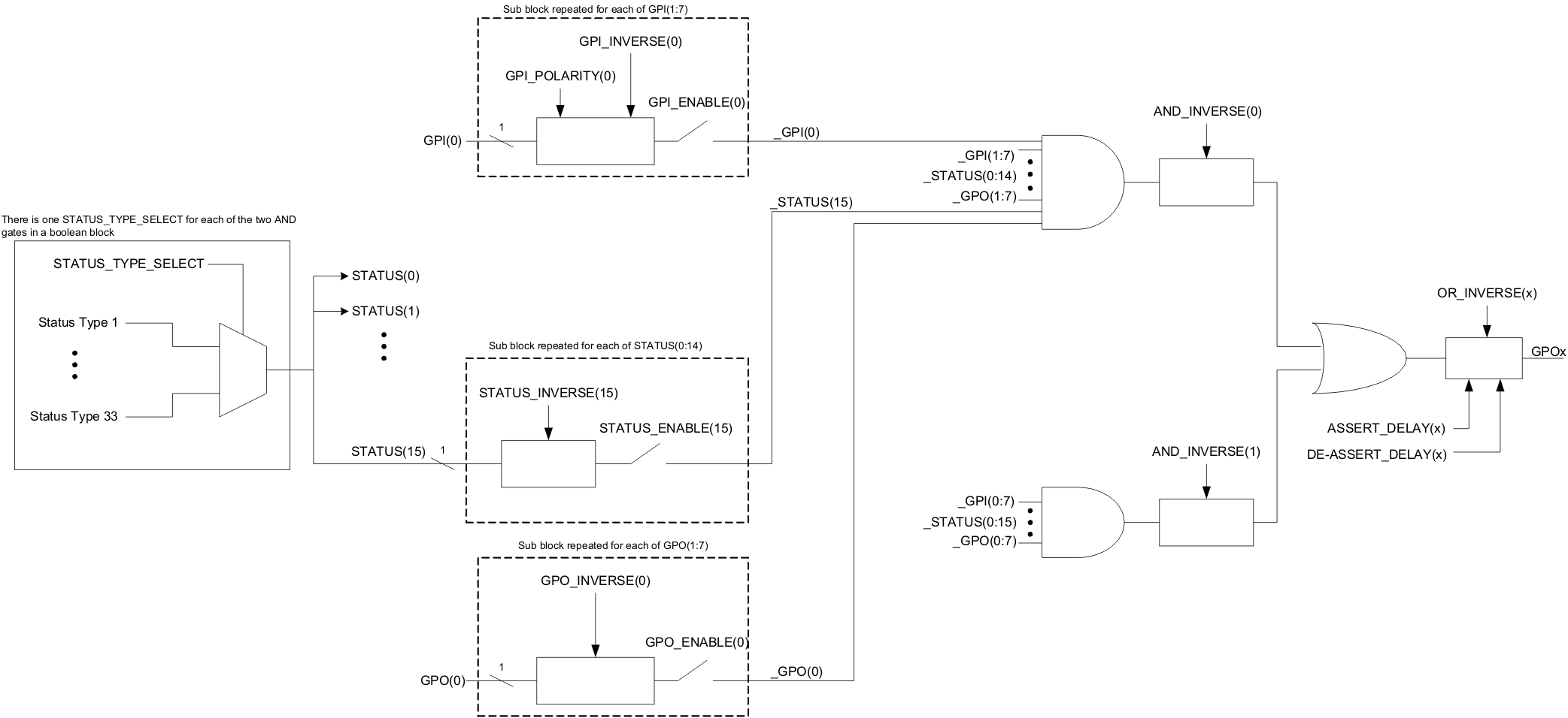
GPIOs can be configured as outputs that are based on Boolean combinations of up to two ANDs, all ORed together (Figure 15). Inputs to the logic blocks can include the first 8 defined GPOs, GPIs and rail-status flags. One rail status type is selectable as an input for each AND gate in a Boolean block. For a selected rail status, the status flags of all active rails can be included as inputs to the AND gate. _LATCH rail-status types stay asserted until cleared by a MFR PMBus command or by a specially configured GPI pin. The different rail-status types are shown in Table 5. See the UCD90xxx Sequencer and System Health Controller PMBus Command Reference for complete definitions of rail-status types. The GPO response can be configured to have a delayed assertion or deassertion. The first 8 GPOs can be chosen as Rail Sequence on/off Dependency. The logic state of the GPO instead of actual pin output is used as dependency condition.
 Figure 15. Boolean Logic Combinations
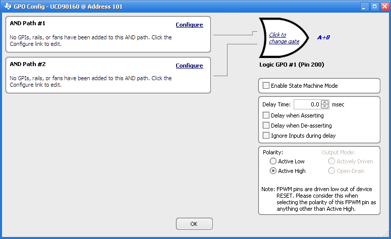
  Figure 16. Fusion Boolean Logic Builder
 Table 5. Rail-Status Types for Boolean Logic
| Rail-Status Types | ||
|---|---|---|
| POWER_GOOD | TON_MAX_FAULT | VOUT_UV_WARN_LATCH |
| MARGIN_EN | TOFF_MAX_WARN | VOUT_UV_FAULT_LATCH |
| MRG_LOW_nHIGH | SEQ_ON_TIMEOUT | TON_MAX_FAULT_LATCH |
| VOUT_OV_FAULT | SEQ_OFF_TIMEOUT | TOFF_MAX_WARN_LATCH |
| VOUT_OV_WARN | SYSTEM_WATCHDOG_TIMEOUT | SEQ_ON_TIMEOUT_LATCH |
| VOUT_UV_WARN | VOUT_OV_FAULT_LATCH | SEQ_OFF_TIMEOUT_LATCH |
| VOUT_UV_FAULT | VOUT_OV_WARN_LATCH | SYSTEM_WATCHDOG_TIMEOUT_LATCH |
When GPO is set to POWER_GOOD, this POWER_GOOD state is based on the actual voltage measurement on the monitor pins assigned to those rails. For a rail that does not have a monitor pin, or have a monitor pin but without voltage monitoring, its POWER_GOOD state is used by sequencing purpose only, and is not be used by the GPO logic evaluation.