SLVSDD7B August 2016 – March 2022 UCD9090A
PRODUCTION DATA
- 1 Features
- 2 Applications
- 3 Description
- 4 Revision History
- 5 Pin Configuration and Functions
- 6 Specifications
-
7 Detailed Description
- 7.1 Overview
- 7.2 Functional Block Diagram
- 7.3 Feature Description
- 7.4
Device Functional Modes
- 7.4.1 Power Supply Sequencing
- 7.4.2 Pin-Selected Rail States
- 7.4.3 Monitoring
- 7.4.4 Fault Responses and Alert Processing
- 7.4.5 Shut Down All Rails and Sequence On (Resequence)
- 7.4.6 GPIOs
- 7.4.7 GPO Control
- 7.4.8 GPO Dependencies
- 7.4.9 GPI Special Functions
- 7.4.10 Power Supply Enables
- 7.4.11 Cascading Multiple Devices
- 7.4.12 PWM Outputs
- 7.4.13 Programmable Multiphase PWMs
- 7.4.14 Margining
- 7.4.15 Run Time Clock
- 7.4.16 System Reset Signal
- 7.4.17 Watch Dog Timer
- 7.4.18 Data and Error Logging to Flash Memory
- 7.4.19 Brownout Function
- 7.4.20 PMBus Address Selection
- 7.4.21 Device Reset
- 7.4.22 JTAG Interface
- 7.4.23 Internal Fault Management and Memory Error Correction (ECC)
- 7.5 Programming
- 8 Application and Implementation
- 9 Power Supply Recommendations
- 10Layout
- 11Device and Documentation Support
- 12Mechanical, Packaging, and Orderable Information
Package Options
Refer to the PDF data sheet for device specific package drawings
Mechanical Data (Package|Pins)
- RGZ|48
Thermal pad, mechanical data (Package|Pins)
- RGZ|48
Orderable Information
7.4.3.2 Current Monitoring
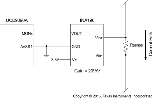
Current can be monitored using the analog inputs. External circuitry, see Figure 7-8, must be used in order to convert the current to a voltage within the range of the UCD9090A MONx input being used.
If a monitor input is configured as a current, the measurements are smoothed by a sliding-average digital filter. The current for 1 rail is measured every 200μs. If the device is programmed to support 10 rails (independent of current not being monitored at all rails), then each rail's current will get measured every 2ms. The current calculation is done with a sliding average using the last 4 measurements. The filter reduces the probability of false fault detections, and introduces a small delay to the current reading. If a rail is defined with a voltage monitor and a current monitor, then monitoring for undercurrent warnings begins once the rail voltage reaches POWER_GOOD_ON. If the rail does not have a voltage monitor, then current monitoring begins after TON_DELAY.
The device supports multiple PMBus commands related to current, including READ_IOUT, which reads external currents from the MON pins; IOUT_OC_FAULT_LIMIT, which sets the overcurrent fault limit; IOUT_OC_WARN_LIMIT, which sets the overcurrent warning limit; and IOUT_UC_FAULT_LIMIT, which sets the undercurrent fault limit. The UCD90xxx Sequencer and System Health Controller PMBus Command Reference contains a detailed description of how current fault responses are implemented using PMBus commands.
IOUT_CAL_GAIN is a PMBus command that allows the scale factor of an external current sensor and any amplifiers or attenuators between the current sensor and the MON pin to be entered by the user in milliohms. IOUT_CAL_OFFSET is the current that results in 0 V at the MON pin. The combination of these PMBus commands allows current to be reported in amperes. The example below using the INA196 would require programming IOUT_CAL_GAIN to Rsense(mΩ)×20.
 Figure 7-8 Current Monitoring Circuit Example Using the INA196