SLRS076A August 2022 – March 2024 ULN2803C
PRODUCTION DATA
- 1
- 1 Features
- 2 Applications
- 3 Description
- 4 Pin Configuration and Functions
- 5 Specifications
- 6 Parameter Measurement Information
- 7 Detailed Description
- 8 Application and Implementation
- 9 Device and Documentation Support
- 10Revision History
- 11Mechanical, Packaging, and Orderable Information
Package Options
Mechanical Data (Package|Pins)
- DW|20
Thermal pad, mechanical data (Package|Pins)
Orderable Information
8.2.2.3 Power Dissipation and Temperature
The number of coils driven is dependent on the coil current and on-chip power dissipation. To determine the number of coils possible, use Equation 2 to calculate ULN2803C on-chip power dissipation PD.
Equation 2. 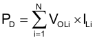
where
- N is the number of channels active together.
- VOLi is the OUTi pin voltage for the load current ILi. This is the same as VCE(SAT).
To ensure the reliability of ULN2803C and the system, the on-chip power dissipation must be lower that or equal to the maximum allowable power dissipation (PD) dictated by Equation 3.
Equation 3. 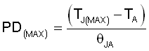
where
- TJ(MAX) is the target maximum junction temperature.
- TA is the operating ambient temperature.
- θJA is the package junction to ambient thermal resistance.
TI recommends to limit the ULN2803C IC die junction temperature to < 125°C. The IC junction temperature is directly proportional to the on-chip power dissipation.