SWRS286 May 2021 WL1801 , WL1831
PRODUCTION DATA
- 1Features
- 2Applications
- 3Description
- 4System Block Diagram
- 5Chip Packaging and Ordering
- 6Mechanical Drawing
Package Options
Mechanical Data (Package|Pins)
- YFV|130
Thermal pad, mechanical data (Package|Pins)
Orderable Information
4 System Block Diagram
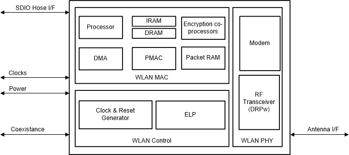
Figure 4-1 shows a system diagrams for the WL18x1.
 Figure 4-1 WL18x1 High-Level Wi-Fi System
Diagram
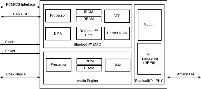
 Figure 4-2 WL1831 High-Level Bluetooth System
Diagram