SLUSC59A April 2015 – December 2016
PRODUCTION DATA.
- 1 Features
- 2 Applications
- 3 Description
- 4 Revision History
- 5 Description (Continued)
- 6 Pin Configuration and Functions
- 7 Specifications
-
8 Detailed Description
- 8.1 Overview
- 8.2 Functional Block Diagram
- 8.3
Feature Description
- 8.3.1 Device Power Up
- 8.3.2 Power Path Management
- 8.3.3 Battery Charging Management
- 8.3.4 Status Outputs (PG, STAT, and INT)
- 8.3.5 Protections
- 8.4 Device Functional Modes
- 8.5 Programming
- 8.6
Register Map
- 8.6.1
I2C Registers
- 8.6.1.1 Input Source Control Register REG00 [reset = 00110xxx, or 3x]
- 8.6.1.2 Power-On Configuration Register REG01 [reset = 00011011, or 0x1B]
- 8.6.1.3 Charge Current Control Register REG02 [reset = 01100000, or 60]
- 8.6.1.4 Pre-Charge/Termination Current Control Register REG03 [reset = 00010001, or 0x11]
- 8.6.1.5 Charge Voltage Control Register REG04 [reset = 10110010, or 0xB2]
- 8.6.1.6 Charge Termination/Timer Control Register REG05 [reset = 11011100, or 0xDC]
- 8.6.1.7 Boost Voltage/Thermal Regulation Control Register REG06 [reset = 01110011, or 0x73]
- 8.6.1.8 Misc Operation Control Register REG07 [reset = 01001011, or 4B]
- 8.6.1.9 System Status Register REG08
- 8.6.1.10 New Fault Register REG09
- 8.6.1.11 Vender / Part / Revision Status Register REG0A
- 8.6.1
I2C Registers
- 9 Application and Implementation
- 10Power Supply Recommendations
- 11Layout
- 12Device and Documentation Support
- 13Mechanical, Packaging, and Orderable Information
Package Options
Mechanical Data (Package|Pins)
- RTW|24
Thermal pad, mechanical data (Package|Pins)
Orderable Information
1 Features
- 90% High Efficiency Switch Mode 3-A Charger
- 3.9-V to 6.2-V Single Input USB-Compliant Charger with 6.4-V Over-Voltage Protection
- Input voltage and current limit supports USB 2.0 and USB 3.0
- Input Current Limit: 100 mA, 150 mA, 500 mA, 900 mA, 1 A, 1.5 A, 2 A, and 3 A
- USB OTG with Adjustable output 4.55 V to 5.5 V at 1 A or 1.5 A
- Fast OTG Startup (22 ms Typ)
- 90% 5-V Boost Mode Efficiency
- Accurate ±15% Hiccup Mode Overcurrent Protection
- Narrow VDC (NVDC) Power Path Management
- Instant System On with No Battery or Deeply Discharged Battery
- Ideal Diode Operation in Battery Supplement Mode
- 1.5-MHz Switching Frequency for Low Profile 1.2-mm Inductor
- I2C port for optimal system performance and status reporting
- Autonomous Battery Charging with or without Host Management
- Battery Charge Enable
- Battery Charge Preconditioning
- Charge Termination and Recharge
- High Accuracy
- ±0.5% Charge Voltage Regulation
- ±7% Charge Current Regulation
- ±7.5% Input Current Regulation
- ±3% Output Voltage Regulation in USB OTG Boost Mode
- High Integration
- Power Path Management
- Synchronous Switching MOSFETs
- Integrated Current Sensing
- Bootstrap Diode
- Internal Loop Compensation
- Safety
- Battery Temperature Sensing for Charging and Discharging in OTG Mode
- Battery Charging Safety Timer
- Thermal Regulation and Thermal Shutdown
- Input and System Over-Voltage Protection
- MOSFET Over-Current Protection
- Charge Status Outputs for LED or Host Processor
- Maximum power tracking capability by input voltage regulation
- 20-µA Low Battery Leakage Current and Support Shipping Mode and System Reset
- I2C Forced BATFET Off with Delay (9 s Typ)
- 4.00-mm x 4.00-mm WQFN-24 Package
2 Applications
- Tablet PC, Smart Phone, Internet Devices
- Portable Audio Speaker
3 Description
The bq24298 is a highly-integrated switch-mode battery charge management and system power path management device for 1 cell Li-Ion and Li-polymer battery in a wide range of smart phone and tablet applications. Its low impedance power path optimizes switch-mode operation efficiency, reduces battery charging time and extends battery life during discharging phase.
Device Information(1)
| PART NUMBER | PACKAGE | BODY SIZE (NOM) |
|---|---|---|
| bq24298 | WQFN (24) | 4.00 mm x 4.00 mm |
- For all available packages, see the orderable addendum at the end of the data sheet.
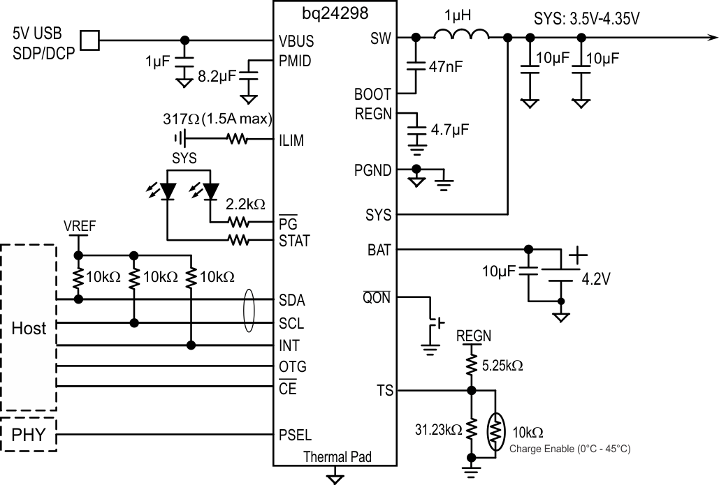
PSEL from PHY, Charging from SDP/DCP, and Optional BATFET Enable Interface

4 Revision History
Changes from * Revision (April 2015) to A Revision
- Changed VREF to VREGN in Figure 16 Go
- Changed 20°C to –20°C and VREF to VREGN in Figure 17 Go
- Changed Equation 1 Go
- Added information to Table 6 Go
- Changed Bit 3 RESET from 1 to 0 in Table 10 Go
- Changed Bit 2 RESET from 1 to 0 in Table 10 Go
- Changed 0 to 1 for REG05 Bit 2 Reset in Table 11 Go
- Changed 1 to 0 for REG05 Bit 1 Reset in Table 11 Go
- Added note to Figure 38 Go
- Changed last paragraph in Output Capacitor sectionGo