SLUSCG5A May 2016 – July 2016
PRODUCTION DATA.
- 1 Features
- 2 Applications
- 3 Description
- 4 Revision History
- 5 Device Comparison Table
- 6 Pin Configuration and Functions
- 7 Specifications
-
8 Detailed Description
- 8.1 Overview
- 8.2 Functional Block Diagram
- 8.3
Feature Description
- 8.3.1 Overvoltage-Protection (OVP) - Continuously Monitored
- 8.3.2 CHG Pin Indication (bq25101, bq25101H)
- 8.3.3 CHG Pin LED Pull-up Source (bq25101, bq25101H)
- 8.3.4 IN-DPM (VIN-DPM or IN-DPM)
- 8.3.5 OUT
- 8.3.6 ISET
- 8.3.7 PRE_TERM - Pre-Charge and Termination Programmable Threshold
- 8.3.8 TS
- 8.3.9 Timers
- 8.3.10 Termination
- 8.4 Device Functional Modes
- 9 Application and Implementation
- 10Power Supply Recommendations
- 11Layout
- 12Device and Documentation Support
- 13Mechanical, Packaging, and Orderable Information
Package Options
Mechanical Data (Package|Pins)
- YFP|6
Thermal pad, mechanical data (Package|Pins)
Orderable Information
1 Features
- Charging
- 1% Charge Voltage Accuracy
- 10% Charge Current Accuracy
- Supports Applications for Very Low Charge Currents - 10 mA to 250 mA
- Supports Minimum 1-mA Charge Termination Current
- Ultra Low Battery Output Leakage Current - Maximum 75 nA
- Adjustable Termination and Precharge Threshold
- High voltage Chemistry Support: 4.30 V
- Protection
- 30-V Input Rating; with 6.5-V Input Overvoltage Protection
- Input Voltage Dynamic Power Management
- 125°C Thermal Regulation; 150°C Thermal Shutdown Protection
- OUT Short-Circuit Protection and ISET Short Detection
- Fixed 10 Hour Safety Timer
- System
- Automatic Termination and Timer Disable Mode (TTDM) for Absent Battery Pack
- Available in Small 1.60 mm × 0.90 mm DSBGA Package
2 Applications
- Fitness Accessories
- Smart Watches
- Bluetooth® Headsets
- Low-Power Handheld Devices
3 Description
The bq25100B device is a highly integrated Li-Ion and Li-Pol linear charger targeted at space-limited portable applications. The high input voltage range with input overvoltage protection supports low-cost unregulated adapters.
The bq25100B has a single power output that charges the battery. A system load can be placed in parallel with the battery as long as the average system load does not keep the battery from charging fully during the 10 hour safety timer.
The battery is charged in three phases: conditioning, constant current and constant voltage. In all charge phases, an internal control loop monitors the IC junction temperature and reduces the charge current if an internal temperature threshold is exceeded.
The charger power stage and charge current sense functions are fully integrated. The charger function has high accuracy current and voltage regulation loops and charge termination. The pre-charge current and termination current threshold are programmed via an external resistor on the bq25100B. The fast charge current value is also programmable via an external resistor.
References to other devices in the bq25100B family are included in this document. For more information on those devices, please see their respective datasheets. This includes references to the CHG pin and the JEITA temperature functionality.
Device Information(1)
| PART NUMBER | PACKAGE | BODY SIZE (NOM) |
|---|---|---|
| bq25100B | DSBGA (6) | 1.60 mm × 0.90 mm |
- For all available packages, see the orderable addendum at the end of the data sheet.
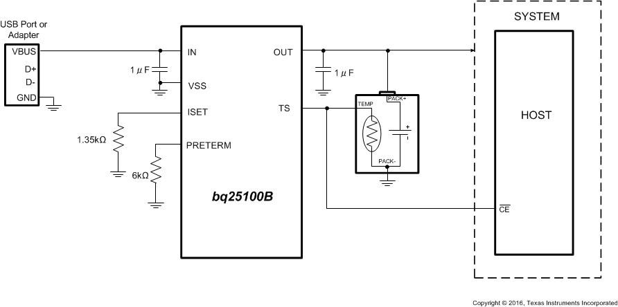
Typical Application Diagram
