SNVS180N April 2002 – April 2016 LM2750
PRODUCTION DATA.
- 1 Features
- 2 Applications
- 3 Description
- 4 Revision History
- 5 Pin Configuration and Functions
- 6 Specifications
- 7 Detailed Description
- 8 Application and Implementation
- 9 Power Supply Recommendations
- 10Layout
- 11Device and Documentation Support
- 12Mechanical, Packaging, and Orderable Information
1 Features
- Wide Input Voltage Range: 2.7 V to 5.6 V
- Inductorless Solution: Application Requires Only Three Small Ceramic Capacitors
- Fixed 5-V Output and Adjustable Output Voltage Options Available
- 85% Peak Efficiency
- 70% Average Efficiency Over Li-Ion Input Range (2.9 V to 4.2 V)
- Output Current up to 120 mA With 2.9 V ≤ VIN ≤ 5.6 V
- Output Current up to 40 mA With 2.7 V ≤ VIN ≤ 2.9 V
- Fixed 1.7-MHz Switching Frequency for a Low-Noise, Low-Ripple Output Signal
- Pre-Regulation Minimizes Input Current Ripple, Keeping the Battery Line
(VIN) Virtually Noise-Free - Shutdown Supply Current Less Than 2 µA
- Tiny WSON Package With Outstanding Power Dissipation: Usually No Derating Required
2 Applications
3 Description
The LM2750 is a regulated switched-capacitor doubler that produces a low-noise output voltage. The 5-V output voltage option (LM2750-5.0) can supply up to 120 mA of output current over a 2.9-V to 5.6-V input range, as well as up to 40 mA of output current when the input voltage is as low as 2.7 V. An adjustable output voltage option with similar output current capabilities is also available (LM2750-ADJ). The LM2750 has been placed in TI's 10-pin WSON, a package with excellent thermal properties that keeps the part from overheating under almost all rated operating conditions.
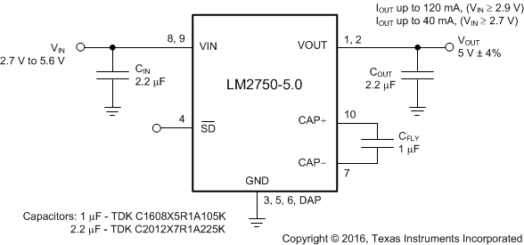
A perfect fit for space-constrained, battery-powered applications, the LM2750 requires only three external components: one input capacitor, one output capacitor, and one flying capacitor. Small, inexpensive ceramic capacitors are recommended for use. In conjunction with the
1.7-MHz fixed switching frequency of the LM2750, these capacitors yield low output-voltage ripple, which is beneficial for systems requiring a low-noise supply. Pre-regulation minimizes input current ripple, thus reducing input noise to negligible levels.
A tightly controlled soft-start feature limits inrush currents during part activation. Shutdown completely disconnects the load from the input. Output current limiting and thermal shutdown circuitry protect both the LM2750 and other connected devices in the event of output shorts or excessive current loads.
Device Information(1)
| PART NUMBER | PACKAGE | BODY SIZE (NOM) |
|---|---|---|
| LM2750 LM2750-ADJ |
WSON (10) | 3.00 mm × 3.00 mm |
- For all available packages, see the orderable addendum at the end of the data sheet.
Typical Application Circuit
