SLPS431B June 2013 – December 2014 CSD22202W15
PRODUCTION DATA.
- 1Features
- 2Applications
- 3Description
- 4Revision History
- 5Specifications
- 6Device and Documentation Support
- 7Mechanical, Packaging, and Orderable Information
Package Options
Refer to the PDF data sheet for device specific package drawings
Mechanical Data (Package|Pins)
- YZF|9
Thermal pad, mechanical data (Package|Pins)
Orderable Information
1 Features
- Low Resistance
- Small Footprint 1.5 mm × 1.5 mm
- Pb Free
- Gate ESD Protection
- RoHS Compliant
- Halogen Free
- Gate-Source Voltage Clamp
2 Applications
- Battery Management
- Battery Protection
- Load Switch Applications
3 Description
The device is designed to deliver the lowest on resistance and gate charge in the smallest outline possible with excellent thermal characteristics in an ultra-low profile. Low on resistance coupled with the small footprint and low profile make the device ideal for battery operated space constrained applications.
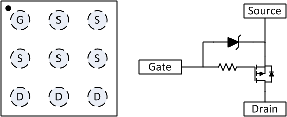
Top View and Circuit Configuration
Product Summary
Ordering Information(1)
| Device | Qty | Media | Package | Ship |
|---|---|---|---|---|
| CSD22202W15 | 3000 | 7-Inch Reel | 1.5 mm × 1.5 mm Wafer BGA Package | Tape and Reel |
| CSD22202W15T | 250 | 7-Inch Reel |
- For all available packages, see the orderable addendum at the end of the data sheet.
Absolute Maximum Ratings
| TA = 25°C unless otherwise stated | VALUE | UNIT | |
|---|---|---|---|
| VDS | Drain-to-Source Voltage | –8 | V |
| VGS | Gate-to-Source Voltage | –6 | V |
| ID | Continuous Drain Current(1)
(Silicon Limitted) |
–10 | A |
| Pulsed Drain Current(2) | –48 | ||
| IG | Continuous Gate Current(3) | –0.5 | A |
| PD | Power Dissipation(1) | 1.5 | W |
| TJ, Tstg |
Operating Junction and Storage Temperature Range |
–55 to 150 | °C |
- RθJA = 75°C/W on 1in2 Cu (2 oz.) on 0.060" thick FR4 PCB.
- Pulse width ≤ 300 µs, duty cycle ≤ 2%
- Limited by gate resistance.
RDS(on) vs VGS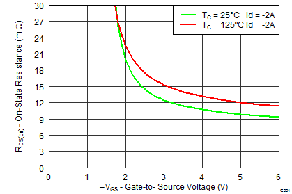 |
Gate Charge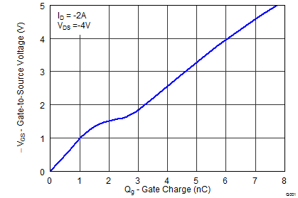 |