SBAS246B December 2001 – November 2014 DAC8532
PRODUCTION DATA.
- 1 Features
- 2 Applications
- 3 Description
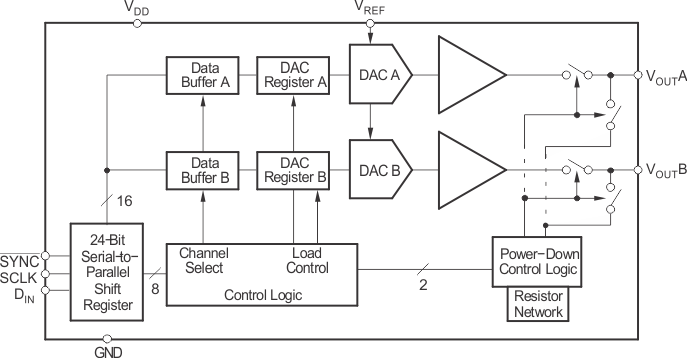
- 4 Simplified Diagram
- 5 Revision History
- 6 Pin Configuration and Functions
- 7 Specifications
- 8 Detailed Description
-
9 Application and Implementation
- 9.1 Application Information
- 9.2 Typical Application
- 10Power Supply Recommendations
- 11Layout
- 12Device and Documentation Support
- 13Mechanical, Packaging, and Orderable Information
Package Options
Mechanical Data (Package|Pins)
- DGK|8
Thermal pad, mechanical data (Package|Pins)
Orderable Information
1 Features
- 16-Bit Monotonic Over Temperature
- MicroPower Operation: 500 µA at 5 V
- Power-On Reset to Zero-Scale
- Power Supply: 2.7 V to 5.5 V
- Settling Time: 10 µs to ±0.003% FSR
- Ultra-Low AC Crosstalk: –100 dB Typ
- Low-Power Serial Interface With
Schmitt-Triggered Inputs - On-Chip Output Buffer Amplifier With Rail-to-Rail Operation
- Double-Buffered Input Architecture
- Simultaneous or Sequential Output Update
and Powerdown - Available in a Tiny VSSOP-8 Package
2 Applications
- Portable Instrumentation
- Closed-Loop Servo Control
- Process Control
- Data Acquisition Systems
- Programmable Attenuation
- PC Peripherals
3 Description
The DAC8532 is a dual channel, 16-bit digital-to-analog converter (DAC) offering low power operation and a flexible serial host interface. Each on-chip precision output amplifier allows rail-to-rail output swing to be achieved over the supply range of 2.7 V to 5.5 V. The device supports a standard 3-wire serial interface capable of operating with input data clock frequencies up to 30 MHz for VDD = 5 V.
The DAC8532 requires an external reference voltage to set the output range of each DAC channel. The device incorporates a power-on reset circuit which ensures that the DAC outputs power up at zero-scale and remain there until a valid write takes place. The DAC8532 provides a flexible power-down feature, accessible over the serial interface, that reduces the current consumption of the device to 200 nA at 5 V.
The low-power consumption of the device in normal operation makes it ideally suited to portable battery-operated equipment and other low-power applications. The power consumption is 2.5 mW at 5 V, reducing to 1 µW in power-down mode.
The DAC8532 is available in a VSSOP-8 package with a specified operating temperature range of –40°C to 105°C.
Device Information(1)
| PART NUMBER | PACKAGE | BODY SIZE (NOM) |
|---|---|---|
| DAC8532 | VSSOP (8) | 3.00 mm × 3.00 mm |
- For all available packages, see the orderable addendum at the end of the datasheet.
4 Simplified Diagram