SLVSAC0F May 2010 – December 2015 DRV8841
PRODUCTION DATA.
- 1 Features
- 2 Applications
- 3 Description
- 4 Revision History
- 5 Pin Configuration and Functions
- 6 Specifications
- 7 Detailed Description
- 8 Application and Implementation
- 9 Power Supply Recommendations
- 10Layout
- 11Device and Documentation Support
- 12Mechanical, Packaging, and Orderable Information
Package Options
Mechanical Data (Package|Pins)
- PWP|28
Thermal pad, mechanical data (Package|Pins)
- PWP|28
Orderable Information
1 Features
- Dual H-Bridge DC Motor Driver
- PWM Control Interface
- Optional Fixed Frequency Current Regulation
- Two Bit Current Control Allows Up to Four Current Levels
- Low MOSFET On-Resistance
- 2.5-A Maximum Drive Current at 24 V and
TA = 25°C - Combined 400 mΩ RDS(ON) of High-Side and Low-Side at 24 V and TA = 25°C
- 2.5-A Maximum Drive Current at 24 V and
- 8.2-V to 45-V Operating Supply Voltage Range
- Low Current Sleep Mode
- Built-In 3.3-V Reference Output
- Thermally Enhanced Surface Mount Package
- Protection Features
- Overcurrent Protection (OCP)
- Thermal Shutdown (TSD)
- Undervoltage Lockout (UVLO)
- Fault Condition Indication Pin (nFAULT)
2 Applications
- Printers
- Scanners
- Office Automation Machines
- Gaming Machines
- Factory Automation
- Robotics
3 Description
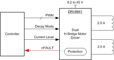
The DRV8841 provides an integrated dual H-bridge motor driver solution for printers, scanners, and other automated equipment applications. The device can be used to drive one or two brushed DC motors, a bipolar stepper motor, or other loads. A simple PWM interface allows easy interfacing to controller circuits.
The output driver block consists of N-channel power MOSFETs configured as H-bridges. The DRV8841 an supply up to 2.5-A peak or 1.75-A RMS output current (with proper heat sinking at 24 V and
TA = 25°C) per H-bridge.
A low-power sleep mode is provided which shuts down internal circuitry to achieve very low quiescent current draw. This sleep mode can be set using a dedicated nSLEEP pin. Internal protection features are provided for overtemperature, overcurrent, and undervoltage. Fault conditions are indicated by a nFAULT pin.
Device Information(1)
| PART NUMBER | PACKAGE | BODY SIZE (NOM) |
|---|---|---|
| DRV8841 | HTSSOP (28) | 9.70 mm × 4.40 mm |
- For all available packages, see the orderable addendum at the end of the data sheet.
Simplified Schematic
