SNLS400D January 2012 – January 2015 DS100BR111A
PRODUCTION DATA.
- 1 Features
- 2 Applications
- 3 Description
- 4 Simplified Schematic
- 5 Revision History
- 6 Pin Configuration and Functions
- 7 Specifications
- 8 Detailed Description
- 9 Application and Implementation
- 10Power Supply Recommendations
- 11Layout
- 12Device and Documentation Support
- 13Mechanical, Packaging, and Orderable Information
Package Options
Mechanical Data (Package|Pins)
- RTW|24
Thermal pad, mechanical data (Package|Pins)
- RTW|24
Orderable Information
1 Features
- Two Channel Repeaters for up to 10.3 Gbps
- DS100BR111 : 1x Bidirectional Lane
- DS100BR210: 2x Unidirectional Channels
- DS100BR111A : 1x Bidirectional Lane
- Low 65 mW/channel (Typical) Power Consumption, with Option to Power Down Unused Channels
- Advanced Signal Conditioning Features
- Receive Equalization up to +36 dB
- Transmit De-emphasis up to -12 dB
- Transmit VOD Control: 600 to 1200 mVp-p
- Low Residual DJ at 10.3 Gbps
- Programmable Via Pin Selection, EEPROM, or SMBus Interface
- Single Supply Voltage: 2.5 V or 3.3 V
- Flow-thru Pinout in 4 mm × 4 mm 24-pin Leadless WQFN Package
- 5 kV HBM ESD Rating
- -40 to 85°C Operating Temperature Range
2 Applications
- High-speed Active Copper Cable Modules in Communication Systems
- 10GE, FC, SAS, SATA 3/6 Gbps (with OOB Detection), InfiniBand, CPRI, RXAUI and many others
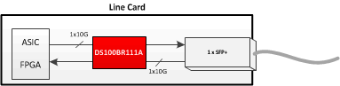
3 Description
The DS100BR111A is an extremely low power, high performance repeater designed to support serial links with data rates up to 10.3 Gbps. The DS100BR111A pinout is configured as one bidirectional lane (one transmit, one receive channel). The DS100BR111A inputs feature a powerful 4-stage continuous time linear equalizer (CTLE) to provide a boost of up to +36 dB at 5 GHz and open an input eye that is completely closed due to inter-symbol interference (ISI) induced by the interconnect mediums such as board traces or twin-axial copper cables. The transmitter features a programmable output de-emphasis driver with up to -12 dB and can drive output voltage levels from 600 mVp-p to 1200 mVp-p.
The programmable settings can be applied via pin control, SMBus protocol, or an external EEPROM. In the EEPROM mode, the configuration information is automatically loaded on power up, thereby eliminating the need for an external microprocessor or software driver. The DS100BR111A consumes just 65 mW/channel (typical), and allows the option to turn off unused channels. This ultra low power consumption eliminates the need for external heat sinks and simplifies thermal management in active cable applications.
Device Information(1)
| PART NUMBER | PACKAGE | BODY SIZE (NOM) |
|---|---|---|
| DS100BR111A | WQFN (24) | 4.00 mm x 4.00 mm |
- For all available packages, see the orderable addendum at the end of the datasheet.
4 Simplified Schematic
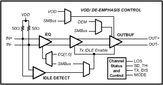
Typical Application